JAJSI40C July 2019 – February 2020 TPS63810 , TPS63811
PRODUCTION DATA.
- 1 特長
- 2 アプリケーション
- 3 概要
- 4 改訂履歴
- 5 デバイス比較表
- 6 Pin Configuration and Functions
- 7 Specifications
-
8 Detailed Description
- 8.1 Overview
- 8.2 Functional Block Diagram
- 8.3
Feature Description
- 8.3.1 Control Scheme
- 8.3.2 Control Scheme
- 8.3.3 Power-Save Mode Operation (PSM)
- 8.3.4 Forced-PWM Operation (FPWM)
- 8.3.5 Ramp-PWM Operation (RPWM)
- 8.3.6 Device Enable (EN)
- 8.3.7 Undervoltage Lockout (UVLO)
- 8.3.8 Soft Start
- 8.3.9 Output Voltage Control
- 8.3.10 Protection Functions
- 8.3.11 Power Good
- 8.3.12 Load Disconnect
- 8.3.13 Output Discharge
- 8.4 Device Functional Modes
- 8.5 Programming
- 8.6
Register Map
- 8.6.1
Register Description
- 8.6.1.1 Register Map
- 8.6.1.2 Register CONTROL (Slave address: 0b1110101; Register address: 0x01; Default: 0x00 or 0x20)
- 8.6.1.3 Register STATUS (Slave address: 0b1110101; Register address: 0x02; Default: 0x00)
- 8.6.1.4 Register DEVID (Slave address: 0b1110101; Register address: 0x03; Default: 0x04)
- 8.6.1.5 Register VOUT1 (Slave address: 0b1110101; Register address: 0x04; Default: 0x3C)
- 8.6.1.6 Register VOUT2 (Slave address: 0b1110101; Register address: 0x05; Default: 0x42)
- 8.6.1
Register Description
- 9 Application and Implementation
- 10Power Supply Recommendations
- 11Layout
- 12デバイスおよびドキュメントのサポート
- 13メカニカル、パッケージ、および注文情報
8.3.8 Soft Start
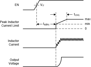
To minimize inrush current and output voltage overshoot during start-up, the device has a soft-start function. At turn on, the switch current limit ramps gradually to its maximum value and the device starts up in a controlled way. The gradual increase of the current limit generates the smallest inrush current for no-load conditions. It is also possible to start into a high load as long as the load does not exceed the device current limit.
The rise time of the output voltage changes with the application circuit and the operating conditions. The output voltage rise time increases if the following occurs:
- The output capacitance is large.
- The load current is large.
- The device operates in boost mode.
See the Application and Implementation section for output voltage rise times in a typical application.
WHITESPACE
 Figure 15. Device Start-Up