JAJSHB0 April 2019 TPS650002-Q1
PRODUCTION DATA.
6.7 Typical Characteristics
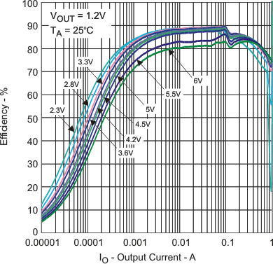 Figure 1. Efficiency (DC-DC 600-mA PFM Mode)
vs Output Current
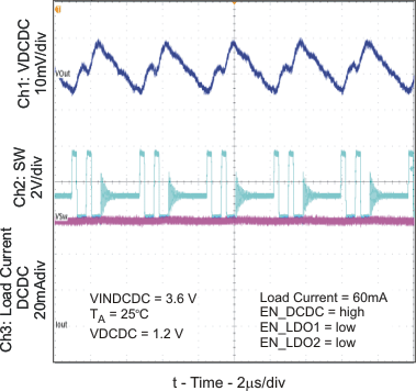 Figure 3. Output Voltage Ripple (DC-DC PFM Mode)
 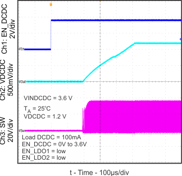 Figure 5. Start-Up Timing (DC-DC)
 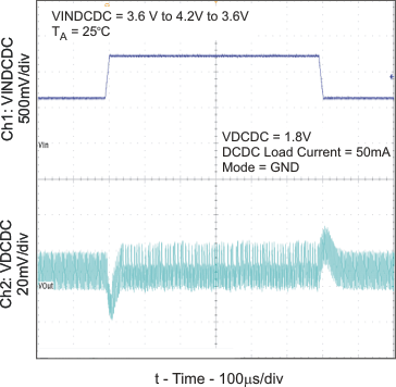 Figure 7. Line Transient Response (DC-DC PFM Mode)
 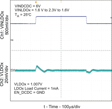 Figure 9. Line Transient Response (LDOx)
  Figure 11. Load Transient Response (DC-DC PWM Mode)
 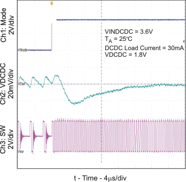 Figure 13. PFM to PWM Transition (DC-DC)
 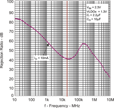 Figure 15. Power-Supply Rejection Ratio (LDOx) vs Frequency
 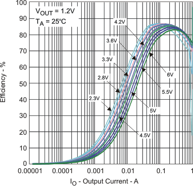 Figure 2. Efficiency (DC-DC 600-mA PWM Mode)
vs Output Current
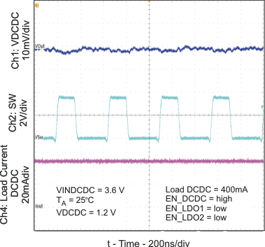 Figure 4. Output Voltage Ripple (DC-DC PWM Mode)
 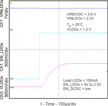 Figure 6. Start-Up Timing (LDOx)
 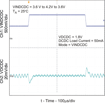 Figure 8. Line Transient Response (DC-DC PWM Mode)
 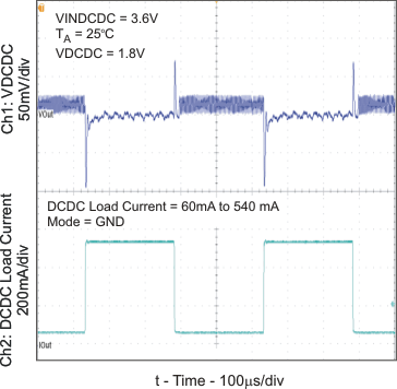 Figure 10. Load Transient Response (DC-DC PFM Mode)
  Figure 12. Load Transient Response (LDOx)
 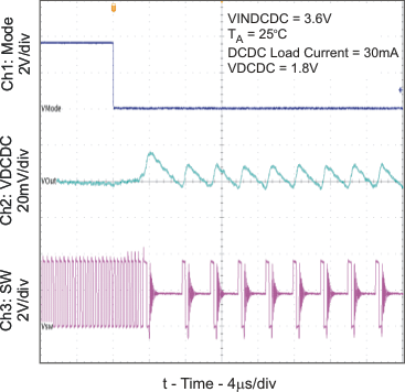 Figure 14. PWM to PFM Transition (DC-DC)