JAJSHB0 April   2019 TPS650002-Q1

PRODUCTION DATA.  

  1. 特長
  2. アプリケーション
  3. 概要
    1.     Device Images
      1.      代表的なアプリケーションの回路図
  4. 改訂履歴
  5. Pin Configuration and Functions
    1.     Pin Functions
  6. Specifications
    1. 6.1 Absolute Maximum Ratings
    2. 6.2 ESD Ratings
    3. 6.3 Recommended Operating Conditions
    4. 6.4 Thermal Information
    5. 6.5 Electrical Characteristics
    6. 6.6 Switching Characteristics
    7. 6.7 Typical Characteristics
  7. Detailed Description
    1. 7.1 Overview
    2. 7.2 Functional Block Diagram
    3. 7.3 Feature Description
      1. 7.3.1 Step-Down Converter
      2. 7.3.2 Soft Start
      3. 7.3.3 Linear Regulators
      4. 7.3.4 Power Good
    4. 7.4 Device Functional Modes
  8. Application and Implementation
    1. 8.1 Application Information
    2. 8.2 Typical Application
      1. 8.2.1 Design Requirements
      2. 8.2.2 Detailed Design Procedure
        1. 8.2.2.1 Output Filter Design (Inductor and Output Capacitor)
          1. 8.2.2.1.1 Inductor Selection
          2. 8.2.2.1.2 Output Capacitor Selection
        2. 8.2.2.2 Input Capacitor Selection
      3. 8.2.3 Application Curves
  9. Power Supply Recommendations
  10. 10Layout
    1. 10.1 Layout Guidelines
    2. 10.2 Layout Examples
  11. 11デバイスおよびドキュメントのサポート
    1. 11.1 デバイス・サポート
      1. 11.1.1 デベロッパー・ネットワークの製品に関する免責事項
    2. 11.2 ドキュメントのサポート
      1. 11.2.1 関連資料
    3. 11.3 ドキュメントの更新通知を受け取る方法
    4. 11.4 コミュニティ・リソース
    5. 11.5 商標
    6. 11.6 静電気放電に関する注意事項
    7. 11.7 Glossary
  12. 12メカニカル、パッケージ、および注文情報

パッケージ・オプション

メカニカル・データ(パッケージ|ピン)
サーマルパッド・メカニカル・データ
発注情報

Pin Configuration and Functions

RTE Package
16-Pin WQFN With Exposed Thermal Pad
Top View
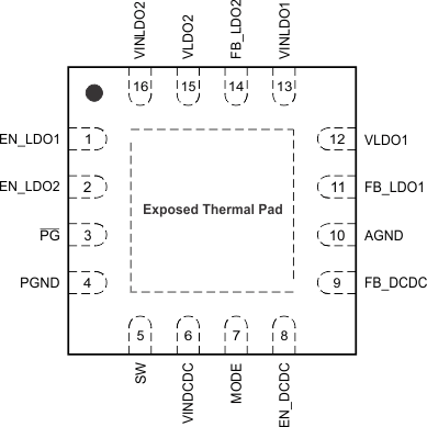
TPS650002-Q1 po_SLVSC45.gif

Pin Functions

PIN I/O DESCRIPTION
NAME NO.
AGND 10 Analog ground – Star back to PGND as close to the IC as possible
EN_DCDC 8 I Enable DC-DC converter
EN_LDO1 1 I Enable LDO1
EN_LDO2 2 I Enable LDO2
FB_DCDC 9 I Voltage to DC-DC error amplifier
FB_LDO1 11 I Voltage to LDO1 error amplifier
FB_LDO2 14 I Voltage to LDO2 error amplifier
MODE 7 I Selects forced-PWM or PWM-to-PFM automatic-transition mode
PG 3 O Open-drain active-low power-good output
PGND 4 Power ground – connected to the thermal pad
SW 5 O Switch pin – connect inductor here
VINDCDC 6 I Input voltage to DC-DC converter and all other control blocks
VINLDO1 13 I Input voltage to LDO1
VINLDO2 16 I Input voltage to LDO2
VLDO1 12 O LDO1 output voltage
VLDO2 15 O LDO2 output voltage
EP Exposed thermal pad