SLVS551A December 2004 – September 2015 TPS65014
PRODUCTION DATA.
- 1 Features
- 2 Applications
- 3 Description
- 4 Revision History
- 5 Pin Configuration and Functions
-
6 Specifications
- 6.1 Absolute Maximum Ratings
- 6.2 ESD Ratings
- 6.3 Recommended Operating Conditions
- 6.4 Thermal Information
- 6.5 Electrical Characteristics
- 6.6 Electrical Characteristics: Battery Charger
- 6.7 Dissipation Ratings
- 6.8 Serial Interface Timing Requirements
- 6.9 Switching Characteristics
- 6.10 Typical Characteristics
-
7 Detailed Description
- 7.1 Overview
- 7.2 Functional Block Diagram
- 7.3 Feature Description
- 7.4 Device Functional Modes
- 7.5
Register Maps
- 7.5.1 CHGSTATUS Register (offset = 01h) (reset: 00h)
- 7.5.2 REGSTATUS Register (offset = 02h) (reset: 00h)
- 7.5.3 MASK1 Register (offset = 03h) (reset: FFh)
- 7.5.4 MASK2 Register (offset = 04h) (reset: FFh)
- 7.5.5 ACKINT1 Register (offset = 05h) (reset: 00h)
- 7.5.6 ACKINT2 Register (offset: 06h) (reset: 00h)
- 7.5.7 CHGCONFIG Register (offset: 07h) (reset: 1Bh)
- 7.5.8 LED1_ON Register (offset: 08h) (reset: 00h)
- 7.5.9 LED1_PER Register (offset: 09h) (reset: 00h)
- 7.5.10 LED2_ON Register (offset: 0Ah) (reset: 00h)
- 7.5.11 LED2_PER (offset: 0Bh) (reset: 00h)
- 7.5.12 VDCDC1 Register (offset: 0Ch) (reset: 32h/33h)
- 7.5.13 VDCDC2 Register (offset: 0Dh) (reset: 60h/70h)
- 7.5.14 VREGS1 Register (offset: 0Eh) (reset: 88h)
- 7.5.15 MASK3 Register (offset: 0Fh) (reset: 00h)
- 7.5.16 DEFGPIO Register (offset = 10h) (reset: 00h)
- 8 Application and Implementation
- 9 Power Supply Recommendations
- 10Layout
- 11Device and Documentation Support
- 12Mechanical, Packaging, and Orderable Information
9 Power Supply Recommendations
9.1 Battery Charger
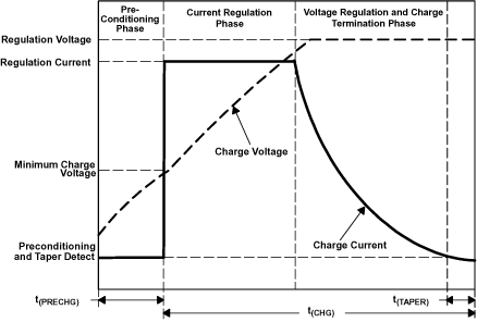
The TPS65014 supports a precision Li-ion or Li-polymer charging system suitable for single cells with either coke or graphite anodes. Charging the battery is possible even without the application processor being powered up. The TPS65014 starts charging when an input voltage on either AC or USB input is present, which is greater than the charger UVLO threshold. See Figure 58 for a typical charge profile.
 Figure 58. Typical Charging Profile
9.1.1 Autonomous Power Source Selection
By default, the TPS65014 attempts to charge from the AC input. If AC input is not present, USB is selected. If both inputs are available, the AC input has priority. The charge current is initially limited to 100 mA when charging from the USB input. This can be increased to 500 mA through the serial interface. The charger can be completely disabled through the interface or from the USB port. The start of the charging process from the USB port is delayed to allow the application processor time to disable USB charging, for instance if a USB OTG port is recognized. The recommended input voltage for charging from the AC input is 4.5 V < VAC < 6.5 V. However, the TPS65014 is capable of withstanding (but not charging from) up to 20 V. Charging is disabled if VAC is greater than typically 7 V.
9.1.2 Temperature Qualification
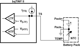
The TPS65014 continuously monitors battery temperature by measuring the voltage between the TS and AGND pins. An internal current source provides the bias for most common 10K negative-temperature coefficient thermistors (NTC) (see Figure 59). The IC compares the voltage on the TS pin against the internal V(LTF) and V(HTF) thresholds to determine if charging is allowed. Once a temperature outside the V(LTF) and V(HTF) thresholds is detected, the IC immediately suspends the charge. The IC suspends charge by turning off the power FET and holding the timer value (that is, timers are not reset). Charge is resumed when the temperature returns to the normal range.
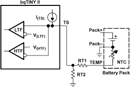
The allowed temperature range for a 103-A T-type thermistor is 0°C to +45°C. However, the user may modify these thresholds by adding two external resistors (see Figure 60).
 Figure 59. TS Pin Configuration
 Figure 60. TS Pin Threshold
9.1.3 Battery Preconditioning
On power up, if the battery voltage is below the V(LOWV) threshold, the TPS65014 applies a precharge current, I(PRECHG), to the battery. This feature revives deeply discharged cells. The charge current during this phase is one tenth of the value in current regulation phase, which is set with IO(out) = KSET × V(SET) / R(SET). The load current in the preconditioning phase must be lower than I(PRECHG) and must allow the battery voltage to rise above V(LOWV) within t(Prechg). VBAT_A is the sense pin to the voltage comparator for the battery voltage. This allows a power-on sense measurement if the VBAT_A and VBAT_B pins are connected together at the battery.
The TPS65014 activates a safety timer, t(PRECHG), during the conditioning phase. If V(LOWV) threshold is not reached within the timer period, the TPS65014 turns off the charger and indicates the fault condition in the CHGSTATUS register. In the case of a fault condition, the TPS65014 reduces the current to I(DETECT). I(DETECT) is used to detect a battery replacement condition. Fault condition is cleared by POR or battery replacement or through the serial interface.
9.1.4 Battery Charge Current
The TPS65014 offers on-chip current regulation. When charging from an AC adapter, a resistor connected between the ISET1 and AGND pins determines the charge rate. A maximum of 1-A charger current from the AC adapter is allowed. When charging from a USB port, either a 100-mA or 500-mA charge rate can be selected through the serial interface; default is 100-mA maximum. Two bits are available in the CHGCONFIG register in the serial interface to reduce the charge current in 25% steps. These only influence charging from the AC input, and may be of use if charging is often suspended due to excessive junction temperature in the TPS65014 (such as at high AC input voltages) and low battery voltages.
9.1.5 Battery Voltage Regulation
The voltage regulation feedback is through the VBAT pin. This pin is tied directly to the positive side of the battery pack. The TPS65014 monitors the battery-pack voltage between the VBAT and AGND pins. The TPS65014 is offered in a fixed-voltage version of 4.2 V.
As a safety backup, the TPS65014 also monitors the charge time in the fast-charge mode. If taper current is not detected within this time period, t(CHG), the TPS65014 turns off the charger and indicates FAULT in the CHGSTATUS register. In the case of a FAULT condition, the TPS65014 reduces the current to I(DETECT). I(DETECT) is used to detect a battery replacement condition. Fault condition is cleared by POR through the serial interface. The safety timer is reset if the TPS65014 is forced out of the voltage regulation mode. The fast-charge timer is disabled by default to allow charging during normal operation of the end equipment. It is enabled through the CHGCONFIG register.
9.1.6 Charge Termination and Recharge
The TPS65014 monitors the charging current during the voltage regulation phase. Once the taper threshold, I(TAPER), is detected, the TPS65014 initiates the taper timer, t(TAPER). Charge is terminated after the timer expires. The TPS65014 resets the taper timer in the event that the charge current returns above the taper threshold, I(TAPER). After a charge termination, the TPS65014 restarts the charge once the voltage on the VBAT pin falls below the V(RCH) threshold. This feature keeps the battery at full capacity at all times. The fast charge timer and the taper timer must be enabled by programming CHGCONFIG(5)=1. A thermal suspend suspends the fast-charge and taper timers.
In addition to the taper current detection, the TPS65014 terminates charge in the event that the charge current falls below the I(TERM) threshold. This feature allows for quick recognition of a battery removal condition. When a full battery is replaced with an empty battery, the TPS65014 detects that the VBAT voltage is below the recharge threshold and starts charging the new battery. The taper and termination bits are cleared in the CHGSTATUS register and if the INT pin is still active due to these two interrupt sources, then it is de-asserted. Depending on the transient seen at the VCC pin, all registers may be set to their default values and require reprogramming with any nondefault values required, such as enabling the fast-charge timer and taper termination; this should only happen if VCC drops below approximately 2 V.
9.1.7 PG Output
The open-drain, power-good (PG) output indicates when a valid power supply is present for the charger. This can be either from the AC adapter input or from the USB. The output turns ON when a valid voltage is detected. A valid voltage is detected whenever the voltage on either pin AC or pin USB rises above the voltage on VBAT plus 100 mV. This output is turned off in the sleep mode. The PG pin can be used to drive an LED or communicate to the host processor. A voltage greater than the V(CHGOVLO) threshold (typ 7-V) at the AC input is not valid and does not activate the PG output. The PG output is held in high impedance state if the charger is in reset by programming CHGCONFIG(6)=1.
The PG output can also be programmed through the LED1_ON and LED1_PER registers in the serial interface. It can then be programmed to be permanently on, off, or to blink with defined on- and period-times. PG is controlled by default through the charger.
9.1.8 Thermal Considerations for Setting Charge Current
The TPS65014 is housed in a 48-pin QFN package with exposed leadframe on the underside. This 7-mm ×
7-mm package exhibits a thermal impedance (junction-to-ambient) of 33 K/W when mounted on a JEDEC high-k board with zero air flow. Refer to Table 33 for maximum charge current considerations.
Table 33. Power Dissipation Limitations
| AMBIENT TEMPERATURE | MAX POWER DISSIPATION FOR Tj = 125°C |
|---|---|
| 25°C | 3 W |
| 55°C | 2.1 W |
| Above 55°C | 30 mW/°C |
Consideration must be given to the maximum charge current when the assembled application board exhibits a thermal impedance, which differs significantly from the JEDEC high-k board. The charger has a thermal shutdown feature, which suspends charging if the TPS65014 junction temperature rises above a threshold of 145°C. This threshold is set 15°C below the threshold used to power down the TPS65014 completely.
9.2 LDO1 Output Voltage Adjustment
The output voltage of LDO1 is set with a resistor divider at the feedback pin. The sum of the two resistors must not exceed 1 MΩ to minimize voltage changes due to leakage current into the feedback pin. The output voltage for LDO1 after start-up is the voltage set by the external resistor divider. It can be reprogrammed with the I2C interface to the three other values defined in the register VREGS1.