SLVSBB2F May   2012  – August 2024 TPS65131-Q1

PRODUCTION DATA  

  1.   1
  2. Features
  3. Applications
  4. Description
  5. Device Comparison
  6. Pin Configuration and Functions
  7. Specifications
    1. 6.1 Absolute Maximum Ratings
    2. 6.2 ESD Ratings
    3. 6.3 Recommended Operating Conditions
    4. 6.4 Thermal Information
    5. 6.5 Electrical Characteristics
    6. 6.6 Switching Characteristics
    7. 6.7 Typical Characteristics
  8. Detailed Description
    1. 7.1 Overview
    2. 7.2 Functional Block Diagram
    3. 7.3 Feature Description
      1. 7.3.1 Power Conversion
      2. 7.3.2 Control
      3. 7.3.3 Output Rails Enable or Disable
      4. 7.3.4 Load Disconnect
      5. 7.3.5 Soft Start
      6. 7.3.6 Overvoltage Protection
      7. 7.3.7 Undervoltage Lockout
      8. 7.3.8 Overtemperature Shutdown
    4. 7.4 Device Functional Modes
      1. 7.4.1 Power-Save Mode
  9. Application and Implementation
    1. 8.1 Application Information
    2. 8.2 Typical Applications
      1. 8.2.1 TPS65131-Q1 With VPOS = 10.5V, VNEG = –10V
      2. 8.2.2 Design Requirements
      3. 8.2.3 Detailed Design Procedure
        1. 8.2.3.1 Programming the Output Voltage
          1. 8.2.3.1.1 Boost Converter
          2. 8.2.3.1.2 Inverting Converter
          3. 8.2.3.1.3 Inductor Selection
        2. 8.2.3.2 Capacitor Selection
          1. 8.2.3.2.1 Input Capacitor
          2. 8.2.3.2.2 Output Capacitors
        3. 8.2.3.3 Rectifier Diode Selection
        4. 8.2.3.4 External P-MOSFET Selection
        5. 8.2.3.5 Stabilizing the Control Loop
          1. 8.2.3.5.1 Feedforward Capacitors
          2. 8.2.3.5.2 Compensation Capacitors
      4. 8.2.4 Analog Supply Input Filter
        1. 8.2.4.1 RC-Filter
        2. 8.2.4.2 LC-Filter
      5. 8.2.5 Thermal Information
      6. 8.2.6 Application Curves
    3. 8.3 Power Supply Recommendations
    4. 8.4 Layout
      1. 8.4.1 Layout Guidelines
      2. 8.4.2 Layout Example
  10. Device and Documentation Support
    1. 9.1 Receiving Notification of Documentation Updates
    2. 9.2 Support Resources
    3. 9.3 Trademarks
    4. 9.4 Electrostatic Discharge Caution
    5. 9.5 Glossary
  11. 10Revision History
  12. 11Mechanical, Packaging, and Orderable Information
    1. 11.1 Mechanical Data
    2. 11.2 Tape and Reel Information

パッケージ・オプション

メカニカル・データ(パッケージ|ピン)
サーマルパッド・メカニカル・データ
発注情報
Boost Converter

An external resistor divider adjusts the output voltage of the TPS65131-Q1 boost converter stage. Connect this divider to the FBP pin. The typical value of the voltage at the FBP pin is the reference voltage, which is 1.213V. The maximum recommended output voltage at the boost converter is 15V. To achieve appropriate accuracy, the current through the feedback divider should be about 100 times higher than the current into the FBP pin. Typical current into the FBP pin is 0.05µA, and the voltage across R2 is 1.213V. Based on those values, the recommended value for R2 should be lower than 200kΩ in order to set the divider current at 5µA or higher.

Calculate the value of resistor R1, as a function of the needed output voltage (VPOS), with Equation 1:

Equation 1. TPS65131-Q1

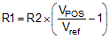
In this example, with R2 = 130kΩ, choose R1 = 1MΩ to set VPOS = 10.5V.