JAJSVA1F May 2012 – August 2024 TPS65131-Q1
PRODUCTION DATA
- 1
- 1 特長
- 2 アプリケーション
- 3 概要
- 4 Device Comparison
- 5 Pin Configuration and Functions
- 6 Specifications
- 7 Detailed Description
-
8 Application and Implementation
- 8.1 Application Information
- 8.2
Typical Applications
- 8.2.1 TPS65131-Q1 With VPOS = 10.5V, VNEG = –10V
- 8.2.2 Design Requirements
- 8.2.3 Detailed Design Procedure
- 8.2.4 Analog Supply Input Filter
- 8.2.5 Thermal Information
- 8.2.6 Application Curves
- 8.3 Power Supply Recommendations
- 8.4 Layout
- 9 Device and Documentation Support
- 10Revision History
- 11Mechanical, Packaging, and Orderable Information
パッケージ・オプション
メカニカル・データ(パッケージ|ピン)
- RGE|24
サーマルパッド・メカニカル・データ
- RGE|24
発注情報
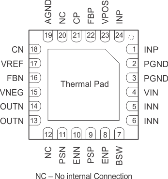
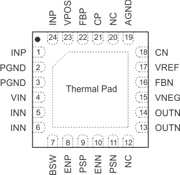
5 Pin Configuration and Functions
 |
 |
|
Figure 5-1 24-pin VQFN Bottom View
|
Figure 5-2 24-pin VQFN
Top View
|
Table 5-1 Pin Functions
| PIN | I/O | DESCRIPTION | |
|---|---|---|---|
| NAME | NO. | ||
| AGND | 19 | — | Analog ground pin |
| BSW | 7 | O | Gate-control pin for external battery switch. This pin goes low when ENP is set high. |
| CN | 18 | I/O | Compensation pin for inverting converter control |
| CP | 21 | I/O | Compensation pin for boost converter control |
| ENN | 10 | I | Enable pin for the negative-output voltage (0V: disabled, VIN: enabled) |
| ENP | 8 | I | Enable pin for the positive-output voltage (0V: disabled, VIN: enabled) |
| FBN | 16 | I | Feedback pin for the negative-output voltage divider |
| FBP | 22 | I | Feedback pin for the positive-output voltage divider |
| INN | 5, 6 | O | Inverting converter switch pin |
| INP | 1, 24 | O | Boost converter switch pin |
| NC(1) | 12, 20 | — | Not connected |
| OUTN | 13, 14 | I/O | Inverting converter switch output |
| PGND | 2, 3 | — | Power ground pin |
| PSN | 11 | I | Power-save mode enable for inverter stage (0V: disabled, VIN: enabled) |
| PSP | 9 | I | Power-save mode enable for boost converter stage (0V: disabled, VIN: enabled) |
| VIN | 4 | I | Control supply input |
| VNEG | 15 | I | Negative-output voltage-sense input |
| VPOS | 23 | I | Positive-output voltage-sense input |
| VREF | 17 | O | Reference output voltage. Bypass this pin with a 220nF capacitor to ground. Connect the lower resistor of the negative-output voltage divider to this pin. |
| Thermal pad | Thermal pad for thermal performance, connect to PGND | ||
(1) NC - No internal connection