JAJSVA1F May 2012 – August 2024 TPS65131-Q1
PRODUCTION DATA
- 1
- 1 特長
- 2 アプリケーション
- 3 概要
- 4 Device Comparison
- 5 Pin Configuration and Functions
- 6 Specifications
- 7 Detailed Description
-
8 Application and Implementation
- 8.1 Application Information
- 8.2
Typical Applications
- 8.2.1 TPS65131-Q1 With VPOS = 10.5V, VNEG = –10V
- 8.2.2 Design Requirements
- 8.2.3 Detailed Design Procedure
- 8.2.4 Analog Supply Input Filter
- 8.2.5 Thermal Information
- 8.2.6 Application Curves
- 8.3 Power Supply Recommendations
- 8.4 Layout
- 9 Device and Documentation Support
- 10Revision History
- 11Mechanical, Packaging, and Orderable Information
パッケージ・オプション
メカニカル・データ(パッケージ|ピン)
- RGE|24
サーマルパッド・メカニカル・データ
- RGE|24
発注情報
8.2.3.1.3 Inductor Selection
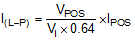
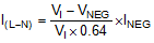
An inductive converter normally requires two main passive components to store energy during the conversion. Therefore, each converter requires an inductor and a storage capacitor. To select the right inductor, it is recommended to keep the possible peak inductor current below the current-limit threshold of the power switch in the chosen configuration. For example, the current-limit threshold of the switch for the boost converter and for the inverting converters is nominally 1950mA. The highest peak current through the switches and the inductor depends on the output load (IPOS, INEG), the input voltage (VI), and the output voltages (VPOS, VNEG). Use Equation 3 to estimate the peak inductor current in the boost converter, I(L-P). Equation 4 shows the corresponding formula for the inverting converter, I(L-N).
The second parameter for choosing the inductor is the desired current ripple in the inductor. Normally, it is advisable to work with a ripple of less than 20% of the average inductor current. A smaller ripple reduces the losses in the inductor, as well as output voltage ripple and EMI. But in the same way, output voltage regulation gets slower, causing higher voltage changes during fast load changes. In addition, a larger inductor usually increases the total system cost. Keep those parameters in mind and calculate the possible inductor value with Equation 5 for the boost converter (L1) and Equation 6 for the inverting converter (L2).
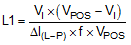
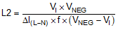
The parameter f is the switching frequency. For the boost converter, ΔI(L-P) is the ripple current in the inductor, that is, 20% of I(L-P). Accordingly, for the inverting converter, ΔI(L-N) is the ripple current in the inductor, that is, 20% of I(L-N). VI is the input voltage, which is 3.3V in this example. So, the calculated inductance value for the boost inductor is 5.1µH and for the inverting converter inductor is 5.1µH. With these calculated values and the calculated currents, it is possible to choose a suitable inductor.
In typical applications, the recommendation is to choose a 4.7µH inductor. The device is optimized to work with inductance values between 3.3µH and 6.8µH. Nevertheless, operation with higher inductance values may be possible in some applications. Perform detailed stability analysis in this case. Be aware of the possibility that load transients and losses in the circuit can lead to higher currents than estimated in Equation 3 and Equation 4. Also, the losses caused by magnetic hysteresis and conductor resistance are a major parameter for total circuit efficiency.
The following table shows inductors from different suppliers used with the TPS65131-Q1 converter:
| VENDOR(1) | INDUCTOR SERIES |
|---|---|
| EPCOS | B8246284-G4 |
| Wurth Elektronik | 7447789XXX |
| 744031XXX | |
| TDK | VLF3010 |
| VLF4012 | |
| Cooper Electronics Technologies | SD12 |