JAJSI26A November 2019 – February 2021 TPS6521815
PRODUCTION DATA
- 1 特長
- 2 アプリケーション
- 3 概要
- 4 Revision History
- 5 概要 (続き)
- 6 Pin Configuration and Functions
- 7 Specifications
-
8 Detailed Description
- 8.1 Overview
- 8.2 Functional Block Diagram
- 8.3
Feature Description
- 8.3.1
Wake-Up and Power-Up and Power-Down Sequencing
- 8.3.1.1 Power-Up Sequencing
- 8.3.1.2 Power-Down Sequencing
- 8.3.1.3 Strobe 1 and Strobe 2
- 8.3.1.4 Supply Voltage Supervisor and Power-Good (PGOOD)
- 8.3.1.5 Backup Supply Power-Good (PGOOD_BU)
- 8.3.1.6 Internal LDO (INT_LDO)
- 8.3.1.7 Current Limited Load Switches
- 8.3.1.8 LDO1
- 8.3.1.9 Coin Cell Battery Voltage Acquisition
- 8.3.1.10 UVLO
- 8.3.1.11 Power-Fail Comparator
- 8.3.1.12 Battery-Backup Supply Power-Path
- 8.3.1.13 DCDC3 and DCDC4 Power-Up Default Selection
- 8.3.1.14 I/O Configuration
- 8.3.1.15 Push Button Input (PB)
- 8.3.1.16 AC_DET Input (AC_DET)
- 8.3.1.17 Interrupt Pin (INT)
- 8.3.1.18 I2C Bus Operation
- 8.3.1
Wake-Up and Power-Up and Power-Down Sequencing
- 8.4 Device Functional Modes
- 8.5 Programming
- 8.6 Register Maps
- 9 Application and Implementation
- 10Power Supply Recommendations
- 11Layout
- 12Device and Documentation Support
- 13Mechanical, Packaging, and Orderable Information
パッケージ・オプション
メカニカル・データ(パッケージ|ピン)
- RSL|48
サーマルパッド・メカニカル・データ
- RSL|48
発注情報
8.3.1.6 Internal LDO (INT_LDO)
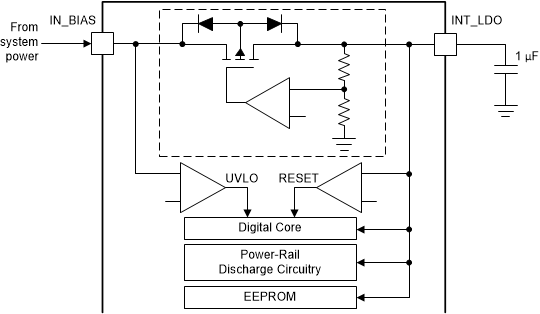
The internal LDO provides a regulated voltage to the internal digital core and analog circuitry. The internal LDO has a nominal output voltage of 2.5 V and can support up to 10 mA of external load. During EEPROM programming, the output voltage is elevated to 3.6 V as described in Section 8.5.1. Therefore, any external circuitry connected to INT_LDO must be capable of supporting that voltage.
When system power fails, the UVLO comparator triggers the power-down sequence. If system power drops below 2.3 V, the digital core is reset and all remaining power rails are shut down instantaneously and are pulled low to ground by their internal discharge circuitry (DCDC1-4 and LDO1).
The internal LDO reverse blocks to prevent the discharging of the output capacitor (CINT_LDO) on the INT_LDO pin. The remaining charge on the INT_LDO output capacitor provides a supply for the power rail discharge circuitry to ensure the outputs are discharged to ground even if the system supply has failed. The amount of hold-up time specified in Section 7.5 is a function of the output capacitor value (CINT_LDO) and the amount of external load on the INT_LDO pin, if any. The design allows for enough hold-up time to sufficiently discharge DCDC1-4, and LDO1 to ensure proper processor power-down sequencing.
 Figure 8-10 Internal LDO and UVLO Sensing