JAJSK46A November 2020 – August 2021 TPS6521845
PRODUCTION DATA
- 1 特長
- 2 アプリケーション
- 3 概要
- 4 Revision History
- 5 Pin Configuration and Functions
- 6 Specifications
-
7 Detailed Description
- 7.1 Overview
- 7.2 Functional Block Diagram
- 7.3
Feature Description
- 7.3.1
Wake-Up and Power-Up and Power-Down Sequencing
- 7.3.1.1 Power-Up Sequencing
- 7.3.1.2 Power-Down Sequencing
- 7.3.1.3 Strobe 1 and Strobe 2
- 7.3.1.4 Supply Voltage Supervisor and Power-Good (PGOOD)
- 7.3.1.5 Backup Supply Power-Good (PGOOD_BU)
- 7.3.1.6 Internal LDO (INT_LDO)
- 7.3.1.7 Current Limited Load Switches
- 7.3.1.8 LDO1
- 7.3.1.9 Coin Cell Battery Voltage Acquisition
- 7.3.1.10 UVLO
- 7.3.1.11 Power-Fail Comparator
- 7.3.1.12 Battery-Backup Supply Power-Path
- 7.3.1.13 DCDC3 and DCDC4 Power-Up Default Selection
- 7.3.1.14 I/O Configuration
- 7.3.1.15 Push Button Input (PB)
- 7.3.1.16 AC_DET Input (AC_DET)
- 7.3.1.17 Interrupt Pin (INT)
- 7.3.1.18 I2C Bus Operation
- 7.3.1
Wake-Up and Power-Up and Power-Down Sequencing
- 7.4 Device Functional Modes
- 7.5 Register Maps
- 8 Application and Implementation
- 9 Power Supply Recommendations
- 10Layout
- 11Device and Documentation Support
- 12Mechanical, Packaging, and Orderable Information
7.3.1.4 Supply Voltage Supervisor and Power-Good (PGOOD)
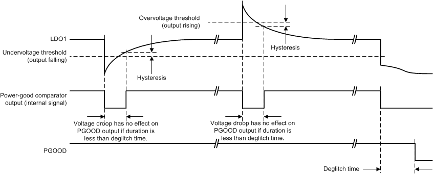
Power-good (PGOOD) is an open-drain output of the built-in voltage supervisor that monitors DCDC1, DCDC2, DCDC3, DCDC4, and LDO1. The output is Hi-Z when all enabled rails are in regulation and driven low when one or more rails encounter a fault which brings the output voltage outside the specified tolerance range. In a typical application PGOOD drives the reset signal of the SOC.
 Figure 7-7 Definition of Undervoltage, Overvoltage Thresholds, Hysteresis, and Deglitch
Times
Figure 7-7 Definition of Undervoltage, Overvoltage Thresholds, Hysteresis, and Deglitch
TimesThe following rules apply to the PGOOD output:
- The power-up default state for THE PGOOD is low. When all rails are disabled, the PGOOD output is driven low.
- Only enabled rails are monitored. Disabled rails are ignored.
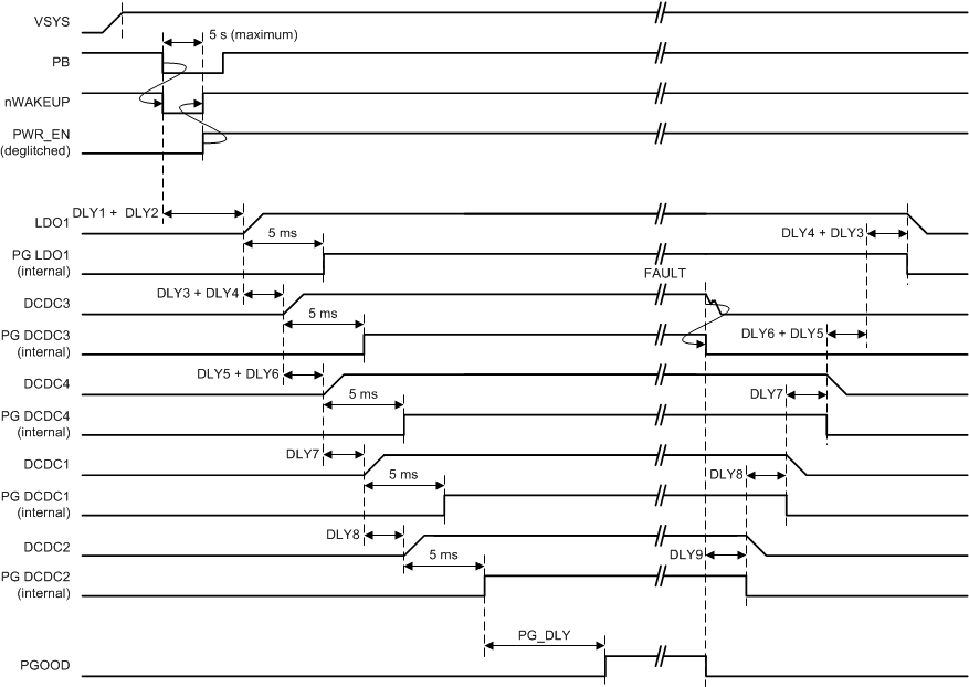
- Power-good monitoring of a particular rail starts 5 ms after the rail is enabled and is continuously monitored thereafter. This allows the rail to power-up.
- The PGOOD is delayed by PGDLY time after the sequencer is finished and the last rail is enabled.
- If an enabled rail is continuously outside the monitoring threshold for longer than the deglitch time, then the PGOOD is pulled low, and all rails are shut-down following the power-down sequence. PGDLY does not apply.
- Disabling a rail manually by resetting the DCx_EN or LDO1_EN bit has no effect on the PGOOD pin. If all rails are disabled, the PGOOD is driven low as the last rail is disabled.
- If the power-down sequencer is triggered, PGOOD is driven low.
- The PGOOD is driven low in the SUSPEND state, regardless of the number of rails that are enabled.
Figure 7-8 shows a typical power-up sequence and PGOOD timing.

A. (1) Sequence shown for TPS65218D0
variant. For other TPS65218xx variants, refer to registers SEQ1-7 in Section
5.6.4 for factory programmed sequence order and timing.
Figure 7-8 Typical
Power-Up Sequence of the Main Output Rails