JAJSK46A November 2020 – August 2021 TPS6521845
PRODUCTION DATA
- 1 特長
- 2 アプリケーション
- 3 概要
- 4 Revision History
- 5 Pin Configuration and Functions
- 6 Specifications
-
7 Detailed Description
- 7.1 Overview
- 7.2 Functional Block Diagram
- 7.3
Feature Description
- 7.3.1
Wake-Up and Power-Up and Power-Down Sequencing
- 7.3.1.1 Power-Up Sequencing
- 7.3.1.2 Power-Down Sequencing
- 7.3.1.3 Strobe 1 and Strobe 2
- 7.3.1.4 Supply Voltage Supervisor and Power-Good (PGOOD)
- 7.3.1.5 Backup Supply Power-Good (PGOOD_BU)
- 7.3.1.6 Internal LDO (INT_LDO)
- 7.3.1.7 Current Limited Load Switches
- 7.3.1.8 LDO1
- 7.3.1.9 Coin Cell Battery Voltage Acquisition
- 7.3.1.10 UVLO
- 7.3.1.11 Power-Fail Comparator
- 7.3.1.12 Battery-Backup Supply Power-Path
- 7.3.1.13 DCDC3 and DCDC4 Power-Up Default Selection
- 7.3.1.14 I/O Configuration
- 7.3.1.15 Push Button Input (PB)
- 7.3.1.16 AC_DET Input (AC_DET)
- 7.3.1.17 Interrupt Pin (INT)
- 7.3.1.18 I2C Bus Operation
- 7.3.1
Wake-Up and Power-Up and Power-Down Sequencing
- 7.4 Device Functional Modes
- 7.5 Register Maps
- 8 Application and Implementation
- 9 Power Supply Recommendations
- 10Layout
- 11Device and Documentation Support
- 12Mechanical, Packaging, and Orderable Information
7.3.1.1 Power-Up Sequencing
When the power-up sequence initiates, STROBE 1 occurs, and any rail assigned to this strobe is enabled. After a delay time of DLY1, STROBE 2 occurs and the rail assigned to this strobe is powered up. The sequence continues until all strobes occur and all DLYx times execute. Strobe assignments and delay times are defined in the SEQx registers, and are changed under I2C control. The power-up sequence executes if one of the following events occurs:
- From the OFF state:
- The push-button (PB) is pressed (falling edge on PB) or
- The AC_DET pin is pulled low (falling edge) or
- The PWR_EN is asserted (driven to high-level) or
- The main power is connected (IN_BIAS) and AC_DET is grounded and
- The device is not in undervoltage lockout (UVLO) or overtemperature shutdown (OTS).
- From the PRE_OFF state:
- The PB is pressed (falling edge on PB) or
- The AC_DET pin is pulled low (falling edge) or
- The PWR_EN is asserted (driven to high-level) and
- The device is not in UVLO or OTS.
- From the SUSPEND state:
- The PB is pressed (falling edge on PB) or
- The AC_DET pin is pulled low (falling edge) or
- The PWR_EN pin is pulled high (level sensitive) and
- The device is not in UVLO or OTS.
When a power-up event is detected, the device enters a WAIT_PWR_EN state and triggers the power-up sequence. The device remains in WAIT_PWR_EN as long as the PWR_EN and either the PB or AC_DET pin are held low. If both, the PB and AC_DET return to logic-high state and the PWR_EN pin has not been asserted within 20 s of entering WAIT_PWR_EN state, the power-down sequence is triggered and the device returns to OFF state. Once PWR_EN is asserted, the device advances to ACTIVE state, which is functionally equivalent to WAIT_PWR_EN. However, the AC_DET pin is ignored and power-down is controlled by the PWR_EN pin only.
Rails not assigned to a strobe (SEQ = 0000b) are not affected by power-up and power-down sequencing and remain in their current ON or OFF state regardless of the sequencer. A rail can be enabled and disabled at any time by setting the corresponding enable bit in the ENABLEx register, with the exception that the ENABLEx register cannot be accessed while the sequencer is active. Enable bits always reflect the current enable state of the rail. For example, the sequencer sets and resets the enable bits for the rails under its control.
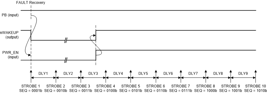
The power-up sequence is defined by strobes and delay times, and can be triggered by the PB, AC_DET (not shown, same as PB), or PWR_EN pin.

 Figure 7-2 Power-Up
Sequences from SUSPEND State; PWR_EN is Power-Up Event
 Figure 7-3 Power-Up
Sequences from RECOVERY State