JAJSK46A November 2020 – August 2021 TPS6521845
PRODUCTION DATA
- 1 特長
- 2 アプリケーション
- 3 概要
- 4 Revision History
- 5 Pin Configuration and Functions
- 6 Specifications
-
7 Detailed Description
- 7.1 Overview
- 7.2 Functional Block Diagram
- 7.3
Feature Description
- 7.3.1
Wake-Up and Power-Up and Power-Down Sequencing
- 7.3.1.1 Power-Up Sequencing
- 7.3.1.2 Power-Down Sequencing
- 7.3.1.3 Strobe 1 and Strobe 2
- 7.3.1.4 Supply Voltage Supervisor and Power-Good (PGOOD)
- 7.3.1.5 Backup Supply Power-Good (PGOOD_BU)
- 7.3.1.6 Internal LDO (INT_LDO)
- 7.3.1.7 Current Limited Load Switches
- 7.3.1.8 LDO1
- 7.3.1.9 Coin Cell Battery Voltage Acquisition
- 7.3.1.10 UVLO
- 7.3.1.11 Power-Fail Comparator
- 7.3.1.12 Battery-Backup Supply Power-Path
- 7.3.1.13 DCDC3 and DCDC4 Power-Up Default Selection
- 7.3.1.14 I/O Configuration
- 7.3.1.15 Push Button Input (PB)
- 7.3.1.16 AC_DET Input (AC_DET)
- 7.3.1.17 Interrupt Pin (INT)
- 7.3.1.18 I2C Bus Operation
- 7.3.1
Wake-Up and Power-Up and Power-Down Sequencing
- 7.4 Device Functional Modes
- 7.5 Register Maps
- 8 Application and Implementation
- 9 Power Supply Recommendations
- 10Layout
- 11Device and Documentation Support
- 12Mechanical, Packaging, and Orderable Information
7.3.1.3 Strobe 1 and Strobe 2
STROBE 1 and STROBE 2 are dedicated to DCDC5 and DCDC6 which are always-on; powered up as soon as the device exits the OFF state, and ON in any other state. STROBE 1 and STROBE 2 options are available only for DCDC5 and DCDC6, not for any other rails.
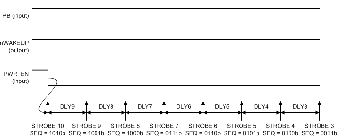
 Figure 7-4 Power-Down Sequences to OFF State; PWR_EN is Power-Down Event; FSEAL = 0b
STROBE2 and
STROBE1 are not shown.
Figure 7-5 Power-Down Sequences to SUSPEND State; PWR_EN is Power-Down Event; FSEAL = 1b
STROBE2 and
STROBE1 are not shown.
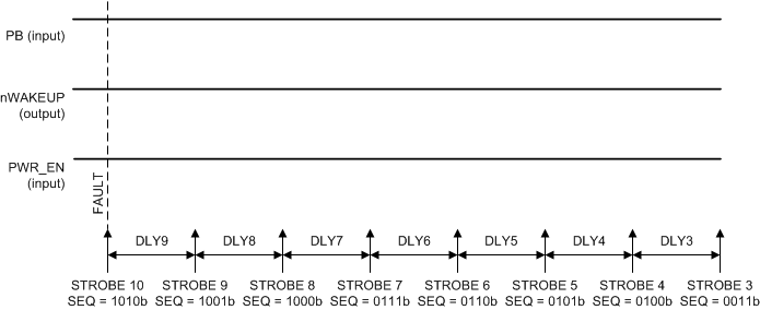
Figure 7-6 Power-Down Sequences to RECOVERY State; TSD or UV is Power-Down Event