JAJSK46A November   2020  – August 2021 TPS6521845

PRODUCTION DATA  

  1. 特長
  2. アプリケーション
  3. 概要
    1.     4
  4. Revision History
  5. Pin Configuration and Functions
  6. Specifications
    1. 6.1 Absolute Maximum Ratings
    2. 6.2 ESD Ratings
    3. 6.3 Recommended Operating Conditions
    4. 6.4 Thermal Information
    5. 6.5 Electrical Characteristics
    6. 6.6 Timing Requirements
    7. 6.7 Typical Characteristics
  7. Detailed Description
    1. 7.1 Overview
    2. 7.2 Functional Block Diagram
    3. 7.3 Feature Description
      1. 7.3.1 Wake-Up and Power-Up and Power-Down Sequencing
        1. 7.3.1.1  Power-Up Sequencing
        2. 7.3.1.2  Power-Down Sequencing
        3. 7.3.1.3  Strobe 1 and Strobe 2
        4. 7.3.1.4  Supply Voltage Supervisor and Power-Good (PGOOD)
        5. 7.3.1.5  Backup Supply Power-Good (PGOOD_BU)
        6. 7.3.1.6  Internal LDO (INT_LDO)
        7. 7.3.1.7  Current Limited Load Switches
          1. 7.3.1.7.1 Load Switch 1 (LS1)
          2. 7.3.1.7.2 Load Switch 2 (LS2)
          3. 7.3.1.7.3 Load Switch 3 (LS3)
        8. 7.3.1.8  LDO1
        9. 7.3.1.9  Coin Cell Battery Voltage Acquisition
        10. 7.3.1.10 UVLO
        11. 7.3.1.11 Power-Fail Comparator
        12. 7.3.1.12 Battery-Backup Supply Power-Path
        13. 7.3.1.13 DCDC3 and DCDC4 Power-Up Default Selection
        14. 7.3.1.14 I/O Configuration
          1. 7.3.1.14.1 Configuring GPO2 as Open-Drain Output
          2. 7.3.1.14.2 Using GPIO3 as Reset Signal to DCDC1 and DCDC2
        15. 7.3.1.15 Push Button Input (PB)
          1. 7.3.1.15.1 Signaling PB-Low Event on the nWAKEUP Pin
          2. 7.3.1.15.2 Push Button Reset
        16. 7.3.1.16 AC_DET Input (AC_DET)
        17. 7.3.1.17 Interrupt Pin (INT)
        18. 7.3.1.18 I2C Bus Operation
    4. 7.4 Device Functional Modes
      1. 7.4.1 Modes of Operation
      2. 7.4.2 OFF
      3. 7.4.3 ACTIVE
      4. 7.4.4 SUSPEND
      5. 7.4.5 RESET
    5. 7.5 Register Maps
  8. Application and Implementation
    1. 8.1 Application Information
      1. 8.1.1 Applications Without Battery Backup Supplies
    2. 8.2 Typical Application
      1. 8.2.1 Design Requirements
      2. 8.2.2 Detailed Design Procedure
        1. 8.2.2.1 Output Filter Design
        2. 8.2.2.2 Inductor Selection for Buck Converters
        3. 8.2.2.3 Output Capacitor Selection
      3. 8.2.3 Application Curves
  9. Power Supply Recommendations
  10. 10Layout
    1. 10.1 Layout Guidelines
    2. 10.2 Layout Example
  11. 11Device and Documentation Support
    1. 11.1 Documentation Support
      1. 11.1.1 Related Documentation
    2. 11.2 Receiving Notification of Documentation Updates
    3. 11.3 サポート・リソース
    4. 11.4 Trademarks
    5. 11.5 静電気放電に関する注意事項
    6. 11.6 用語集
  12. 12Mechanical, Packaging, and Orderable Information

パッケージ・オプション

メカニカル・データ(パッケージ|ピン)
サーマルパッド・メカニカル・データ
発注情報

Application Curves

at TJ = 25°C unless otherwise noted
at TJ = 25°C unless otherwise notedGUID-555D36FF-6A47-4225-B6A6-26F5566CAB59-low.gif
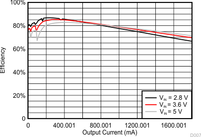
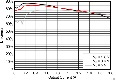
VOUT = 1.1 V
Figure 8-3 DCDC1/DCDC2 Efficiency. at TJ = 25°C unless otherwise noted
GUID-9BF8E563-CC00-4B12-BD23-3FD166E596CC-low.gif
VOUT = 1.5 V
Figure 8-5 DCDC3 Efficiency
GUID-C5BFFD6C-3EA6-4DEC-BA61-AD01FD13B74B-low.gif
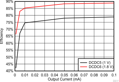
IN_BU = 0 V CC = 3 V
Figure 8-7 DCDC5/DCDC6 Efficiency
GUID-DA4B306F-7CE7-4E12-B1CA-C87B4F57CD93-low.gif
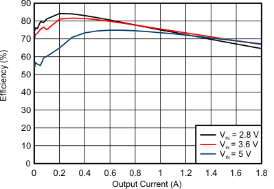
VOUT = 1.2 V
Figure 8-4 DCDC3 Efficiency
GUID-994921F8-4D04-49FA-83FF-1D0597C8E6DB-low.gif
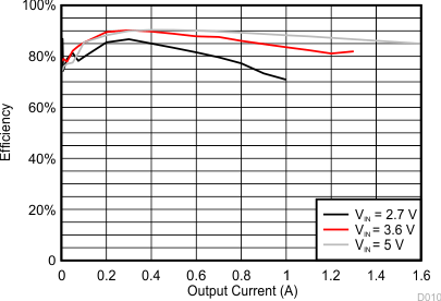
VOUT = 3.3 V
Figure 8-6 DCDC4 Efficiency