JAJSCX2F january 2017 – may 2023 TPS65235-1
PRODUCTION DATA
- 1
- 1 特長
- 2 アプリケーション
- 3 概要
- 4 Revision History
- 5 Pin Configuration and Functions
- 6 Specifications
-
7 Detailed Description
- 7.1 Overview
- 7.2 Functional Block Diagram
- 7.3
Feature Description
- 7.3.1 Boost Converter
- 7.3.2 Linear Regulator and Current Limit
- 7.3.3 Boost Converter Current Limit
- 7.3.4 Charge Pump
- 7.3.5 Slew Rate Control
- 7.3.6 Short-Circuit Protection, Hiccup, and Overtemperature Protection
- 7.3.7 Tone Generation
- 7.3.8 Tone Detection
- 7.3.9 Audio Noise Rejection
- 7.3.10 Disable and Enable
- 7.3.11 Component Selection
- 7.4 Device Functional Modes
- 7.5 Programming
- 7.6 Register Maps
- 8 Application and Implementation
- 9 Device and Documentation Support
- 10Mechanical, Packaging, and Orderable Information
パッケージ・オプション
メカニカル・データ(パッケージ|ピン)
- RUK|20
サーマルパッド・メカニカル・データ
- RUK|20
発注情報
7.3.7 Tone Generation
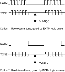
A 22-kHz tone signal is implemented at the LNB output voltage as a carrier for DiSEqC command. This tone signal can be generated by feeding an external 22-kHz clock at the EXTM pin, and it can also be generated with its internal tone generator controlled by EXTM pin. If EXTM pin is toggled to high, the internal tone signal will be superimposed at the LNB output, if EXTM pin is low, there will be no tone superimposed at the output stage of the regulator facilitates a push-pull circuit, so even at zero loading; the 22-kHz tone at the output is still clean without distortion.
There are two ways to generate the 22-kHz tone signal at the output.
For option1, if the EXTM has 44-kHz tone input, and the bit EXTM TONE of the Control Register 1 is set to 1b, the LNB tone output is 44 kHz.
 Figure 7-2 Two Ways to Generate 22-kHz tone