JAJSCX2F january 2017 – may 2023 TPS65235-1
PRODUCTION DATA
- 1
- 1 特長
- 2 アプリケーション
- 3 概要
- 4 Revision History
- 5 Pin Configuration and Functions
- 6 Specifications
-
7 Detailed Description
- 7.1 Overview
- 7.2 Functional Block Diagram
- 7.3
Feature Description
- 7.3.1 Boost Converter
- 7.3.2 Linear Regulator and Current Limit
- 7.3.3 Boost Converter Current Limit
- 7.3.4 Charge Pump
- 7.3.5 Slew Rate Control
- 7.3.6 Short-Circuit Protection, Hiccup, and Overtemperature Protection
- 7.3.7 Tone Generation
- 7.3.8 Tone Detection
- 7.3.9 Audio Noise Rejection
- 7.3.10 Disable and Enable
- 7.3.11 Component Selection
- 7.4 Device Functional Modes
- 7.5 Programming
- 7.6 Register Maps
- 8 Application and Implementation
- 9 Device and Documentation Support
- 10Mechanical, Packaging, and Orderable Information
パッケージ・オプション
メカニカル・データ(パッケージ|ピン)
- RUK|20
サーマルパッド・メカニカル・データ
- RUK|20
発注情報
7.3.11.2 Capacitor Selection
The TPS65235-1 device has a 1-MHz nonsynchronous boost converter integrated and the boost converter features the internal compensation network. The TPS65235-1 device works well with both ceramic capacitor and electrolytic capacitor.
The recommended ceramic capacitors for the TPS65235-1 application are, at the minimum, rated as X7R/X5R, with a 35-V rating, and a 1206 size for the achieving lower LNB output ripple. Table 7-1 lists the recommended ceramic capacitors list for both 4.7-µH and 10-µH boost inductors.
If more cost-effictive design is needed, use a 100-µF electrolytic (low ESR) and a 10-µF or 35-V ceramic capacitor.
| BOOST INDUCTOR | CAPACITORS | TOLERANCE (%) | RATING (V) | SIZE |
|---|---|---|---|---|
| 10 µH | 2 × 22 µF | ±10 | 35 | 1206 |
| 2 × 10 µF | ±10 | 35 | 1206 | |
| 4.7 µH | 2 × 22 µF | ±10 | 35 | 1206 |
| 2 × 10 µF | ±10 | 35 | 1206 | |
| 22 µF | ±10 | 35 | 1206 |
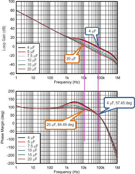
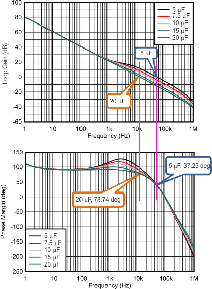
Figure 7-6 and Figure 7-7 show a bode plot of boost loop with 4.7-µH and 10-µH inductance and 4 µF, 5 µF, 7.5 µF, 10 µF, 15 µF, and 20 µF of boost capacitance after degrading. As the boost capacitance increases, the phase margin increases.
 Figure 7-6 Gain and Phase Margin of the Boost Loop With Different Boost Capacitance (VIN = 12 V, VOUT = 18.2 V, ILOAD = 1 A, fSW = 1 MHz, 4.7 µH, Typical Bode Plot)
 Figure 7-7 Gain and Phase Margin of
the Boost Loop With Different Boost Capacitance (VIN = 12 V,
VOUT = 18.2 V, ILOAD = 1 A,
fSW = 1 MHz, 10 µH, Typical Bode Plot)