JAJSI91D december 2019 – may 2023 TPS652353
PRODUCTION DATA
- 1
- 1 特長
- 2 アプリケーション
- 3 概要
- 4 Revision History
- 5 Pin Configuration and Functions
- 6 Specifications
-
7 Detailed Description
- 7.1 Overview
- 7.2 Functional Block Diagram
- 7.3
Feature Description
- 7.3.1 Boost Converter
- 7.3.2 Linear Regulator and Current Limit
- 7.3.3 Boost Converter Current Limit
- 7.3.4 Charge Pump
- 7.3.5 Slew Rate Control
- 7.3.6 Short Circuit Protection, Hiccup and Overtemperature Protection
- 7.3.7 Tone Generation
- 7.3.8 Tone Detection
- 7.3.9 Audio Noise Rejection
- 7.3.10 Disable and Enable
- 7.3.11 Component Selection
- 7.4 Device Functional Modes
- 7.5 Programming
- 7.6 Register Maps
- 8 Application and Implementation
- 9 Device and Documentation Support
- 10Mechanical, Packaging, and Orderable Information
パッケージ・オプション
メカニカル・データ(パッケージ|ピン)
- RUK|20
サーマルパッド・メカニカル・データ
- RUK|20
発注情報
7.3.11.2 Capacitor Selection
The TPS652353 device has a 1-MHz nonsynchronous boost converter integrated and the boost converter features the internal compensation network. The TPS652353 device works well with both ceramic capacitor and electrolytic capacitor.
The recommended ceramic capacitors for the TPS652353 application are, at the minimum, rated as X7R/X5R, with a 35-V rating, and a 1206 size for the achieving lower LNB output ripple. Table 7-1 lists the recommended ceramic capacitors list for both 4.7-µH and 10-µH boost inductors.
If more cost-effictive design is needed, use a 100-µF electrolytic (low ESR) and a 10-µF or 35-V ceramic capacitor.
| BOOST INDUCTOR | CAPACITORS | TOLERANCE (%) | RATING (V) | SIZE |
|---|---|---|---|---|
| 10 µH | 2 × 22 µF | ±10 | 35 | 1206 |
| 2 × 10 µF | ±10 | 35 | 1206 | |
| 4.7 µH | 2 × 22 µF | ±10 | 35 | 1206 |
| 2 × 10 µF | ±10 | 35 | 1206 | |
| 22 µF | ±10 | 35 | 1206 |
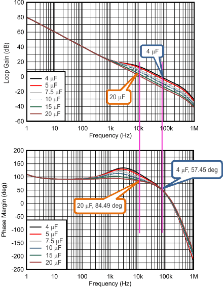
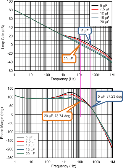
Figure 7-6 and Figure 7-7 show a bode plot of boost loop with 4.7-µH and 10-µH inductance and 4 µF, 5 µF, 7.5 µF, 10 µF, 15 µF, and 20 µF of boost capacitance after degrading. As the boost capacitance increases, the phase margin increases.
 Figure 7-6 Gain and Phase Margin of the Boost Loop With Different Boost Capacitance
(VIN = 12 V, VOUT = 18.2 V, ILOAD = 1 A, fSW = 1 MHz, 4.7 µH, Typical Bode Plot)
 Figure 7-7 Gain and Phase Margin of the Boost Loop With Different Boost Capacitance
(VIN = 12 V, VOUT =18.2 V, ILOAD = 1 A, fSW = 1 MHz, 10 µH, Typical Bode Plot)