JAJSI91D december 2019 – may 2023 TPS652353
PRODUCTION DATA
- 1
- 1 特長
- 2 アプリケーション
- 3 概要
- 4 Revision History
- 5 Pin Configuration and Functions
- 6 Specifications
-
7 Detailed Description
- 7.1 Overview
- 7.2 Functional Block Diagram
- 7.3
Feature Description
- 7.3.1 Boost Converter
- 7.3.2 Linear Regulator and Current Limit
- 7.3.3 Boost Converter Current Limit
- 7.3.4 Charge Pump
- 7.3.5 Slew Rate Control
- 7.3.6 Short Circuit Protection, Hiccup and Overtemperature Protection
- 7.3.7 Tone Generation
- 7.3.8 Tone Detection
- 7.3.9 Audio Noise Rejection
- 7.3.10 Disable and Enable
- 7.3.11 Component Selection
- 7.4 Device Functional Modes
- 7.5 Programming
- 7.6 Register Maps
- 8 Application and Implementation
- 9 Device and Documentation Support
- 10Mechanical, Packaging, and Orderable Information
パッケージ・オプション
メカニカル・データ(パッケージ|ピン)
- RUK|20
サーマルパッド・メカニカル・データ
- RUK|20
発注情報
7.3.2 Linear Regulator and Current Limit
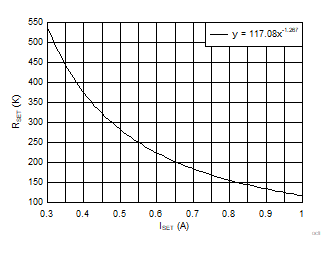
The linear regulator is used to generate the 22-kHz tone signal by changing the LDO reference voltage. The linear regulator features low-dropout voltage to minimize power loss while maintaining enough head room for the 22-kHz tone with 650-mV amplitude. The linear regulator also implements a tight current limit for overcurrent protection. The current limit is set by an external resistor connected to ISET pin. Linear Regulator Current Limit Vs Resistor shows the relationship between the current limit threshold and the resistor value.
 Figure 7-1 Linear Regulator Current Limit Vs Resistor
A 200-kΩ resistor sets the current to 0.65 A, and 110-kΩ resistor sets the current to approximately 1 A.