JAJSQ69B december   2015  – may 2023 TPS65265

PRODUCTION DATA  

  1.   1
  2. 特長
  3. アプリケーション
  4. 概要
  5. Revision History
  6. Device Comparison Table
  7. Pin Configuration and Functions
  8. Specifications
    1. 7.1 Absolute Maximum Ratings
    2. 7.2 ESD Ratings
    3. 7.3 Recommended Operating Conditions
    4. 7.4 Thermal Information
    5. 7.5 Electrical Characteristics
    6. 7.6 Typical Characteristics
  9. Detailed Description
    1. 8.1 Overview
    2. 8.2 Functional Block Diagram
    3. 8.3 Feature Description
      1. 8.3.1  Adjusting the Output Voltage
      2. 8.3.2  Mix PGOOD, PG_DLY Functions
        1. 8.3.2.1 Programmable PGOOD DELAY
        2. 8.3.2.2 Relay Control
      3. 8.3.3  Enable and Adjusting UVLO
      4. 8.3.4  Soft-Start Time
      5. 8.3.5  Power-Up Sequencing
        1. 8.3.5.1 External Power Sequencing
        2. 8.3.5.2 Automatic Power Sequencing
      6. 8.3.6  V7V Low Dropout Regulator and Bootstrap
      7. 8.3.7  Out of Phase Operation
      8. 8.3.8  Output Overvoltage Protection (OVP)
      9. 8.3.9  PSM
      10. 8.3.10 Slope Compensation
      11. 8.3.11 Overcurrent Protection
        1. 8.3.11.1 High-Side MOSFET Overcurrent Protection
        2. 8.3.11.2 Low-Side MOSFET Overcurrent Protection
      12. 8.3.12 Adjustable Switching Frequency
      13. 8.3.13 Thermal Shutdown
    4. 8.4 Device Functional Modes
      1. 8.4.1 Operation With VIN < 4 V (Minimum VIN)
      2. 8.4.2 Operation With EN Control
  10. Application and Implementation
    1. 9.1 Application Information
    2. 9.2 Typical Application
      1. 9.2.1 Design Requirements
      2. 9.2.2 Detailed Design Procedure
        1. 9.2.2.1 Output Inductor Selection
        2. 9.2.2.2 Output Capacitor Selection
        3. 9.2.2.3 Input Capacitor Selection
        4. 9.2.2.4 Loop Compensation
      3. 9.2.3 Application Curves
    3. 9.3 Power Supply Recommendations
    4. 9.4 Layout
      1. 9.4.1 Layout Guidelines
      2. 9.4.2 Layout Example
  11. 10Device and Documentation Support
    1. 10.1 ドキュメントの更新通知を受け取る方法
    2. 10.2 サポート・リソース
    3. 10.3 Trademarks
    4. 10.4 静電気放電に関する注意事項
    5. 10.5 用語集
  12. 11Mechanical, Packaging, and Orderable Information

パッケージ・オプション

メカニカル・データ(パッケージ|ピン)
サーマルパッド・メカニカル・データ
発注情報

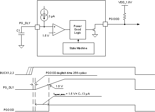
Programmable PGOOD DELAY

An internal 3-µA pullup current source is connected to PG_DLY pin. The PGOOD delay time can be programmed by connecting a capacitor between PG_DLY pin and ground. The delay time can be calculated as Equation 2.

Equation 2. GUID-1947E5DE-80F0-4C71-8ABF-298E85441D40-low.gif

where

  • VPG_DLY = 1.5 V
  • Ip = 3 µA
GUID-89692D05-B412-4F8D-82FC-4ECE03C0166C-low.gifFigure 8-2 Power Good Delay Timing Diagram