JAJSHI2E June 2014 – May 2019 TPS65283 , TPS65283-1
PRODUCTION DATA.
- 1 特長
- 2 アプリケーション
- 3 概要
- 4 代表的な回路図
- 5 改訂履歴
- 6 概要(続き)
- 7 Pin Configuration and Functions
- 8 Specifications
-
9 Detailed Description
- 9.1 Overview
- 9.2 Functional Block Diagram
- 9.3
Feature Description
- 9.3.1 Power Switch Detailed Description
- 9.3.2
Buck DC-DC Converter Detailed Description
- 9.3.2.1 Output Voltage
- 9.3.2.2 Adjustable Switching Frequency
- 9.3.2.3 Synchronization
- 9.3.2.4 Error Amplifier
- 9.3.2.5 Slope Compensation
- 9.3.2.6 Enable and Adjusting UVLO
- 9.3.2.7 Internal V7V Regulator
- 9.3.2.8 Short Circuit Protection
- 9.3.2.9 Bootstrap Voltage (BST) and Low Dropout Operation
- 9.3.2.10 Output Overvoltage Protection (OVP)
- 9.3.2.11 Power Good
- 9.3.2.12 Power-Up Sequencing
- 9.3.2.13 Thermal Performance
- 9.4 Device Functional Modes
- 10Application and Implementation
- 11Power Supply Recommendations
- 12Layout
- 13デバイスおよびドキュメントのサポート
- 14メカニカル、パッケージ、および注文情報
パッケージ・オプション
メカニカル・データ(パッケージ|ピン)
- RGE|24
サーマルパッド・メカニカル・データ
- RGE|24
発注情報
9.3.1.7 Programming the Current-Limit Threshold
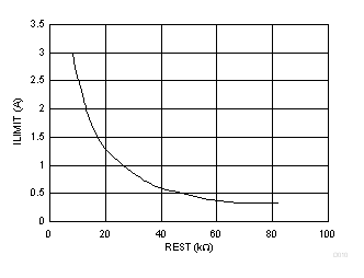
The overcurrent threshold is user programmable through an external resistor. The TPS65283, TPS65283-1 uses an internal regulation loop to provide a regulated voltage on the RLIM pin. The current-limit threshold is proportional to the current sourced out of RSET. The recommended 1% resistor range for RSET is 9.1 kΩ ≤ RLIM ≤ 80.6 kΩ to adjust the current limit of the switch. Many applications require that the minimum current limit is above a certain current level or that the maximum current limit is below a certain current level, so it is important to consider the tolerance of the overcurrent threshold when selecting a value for RLIM. The following equations and Figure 23 can be used to calculate the resulting overcurrent threshold for a given external resistor value (RSET).
Current-Limit Threshold Equations (IOS):
 Figure 23. Current-Limit Threshold vs RLIM