Figure 8-3 through Figure 8-30 apply to the circuit of Figure 8-1. VIN = 12 V. TA = 25°C unless otherwise specified.
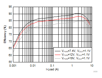 Figure 8-3 VDD2
Efficiency Curve, VOUT = 1.1 V
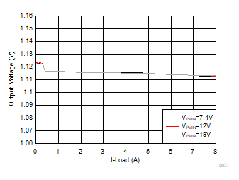 Figure 8-5 VDD2
Load Regulation, VOUT = 1.1 V
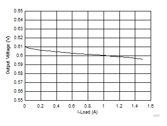 Figure 8-7 VDDQ
Load Regulation, VOUT = 0.6 V
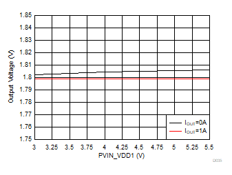 Figure 8-9 VDD1 Line Regulation,
VOUT = 1.8 V
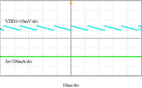 Figure 8-11 VDD1 Output Voltage
Ripple, IOUT = 0 A
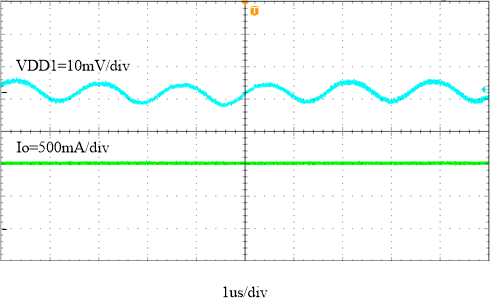 Figure 8-13 VDD1 Output Voltage
Ripple, IOUT = 1 A
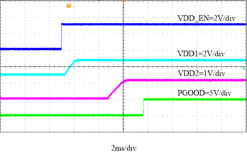 Figure 8-15 Start-Up Through VDD_EN, IVDD1OUT = 1 A, IVDD2OUT = 8
A
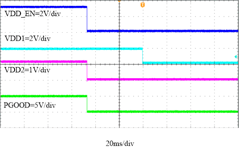 Figure 8-17 Shutdown Through VDD_EN, IVDD1OUT = 1 A, IVDD2OUT = 8
A
| IVDD2OUT = 8 A |
IVDDQ
= 1.5 A |
|
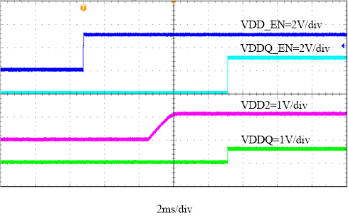
Figure 8-19 VDDQ
Start-Up Through VDDQ_EN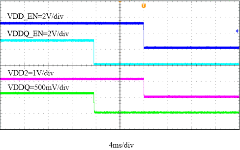
| IVDD2OUT = 8 A |
IVDDQ
= 1.5 A |
|
Figure 8-21 VDDQ
Shutdown Through VDDQ_EN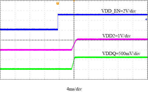
| IVDD2OUT = 8 A |
IVDDQ
= 1.5 A |
|
Figure 8-23 VDDQ
Start-Up Through VDD_EN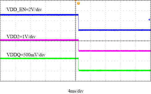
| IVDD2OUT = 8 A |
IVDDQ
= 1.5 A |
|
Figure 8-25 VDDQ
Shutdown Through VDD_EN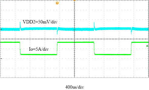 Figure 8-27 VDD2
Transient Response, 1.6 A to 8 A
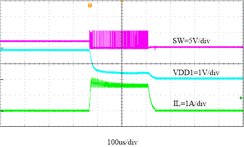 Figure 8-29 VDD1
Normal Operation to Output Hard Short
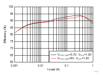 Figure 8-4 VDD1
Efficiency Curve, VOUT = 1.8 V
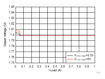 Figure 8-6 VDD1
Load Regulation, VOUT = 1.8 V
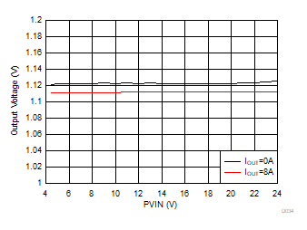 Figure 8-8 VDD2 Line
Regulation,VOUT = 1.1 V
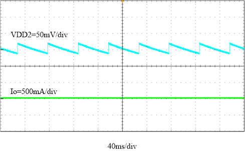 Figure 8-10 VDD2 Output Voltage
Ripple, IOUT = 0 A
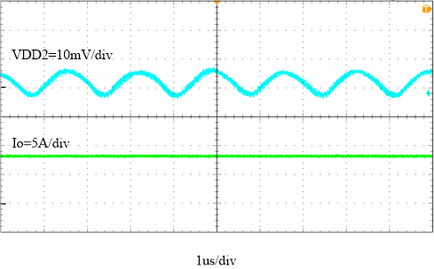 Figure 8-12 VDD2 Output Voltage
Ripple, IOUT = 8 A
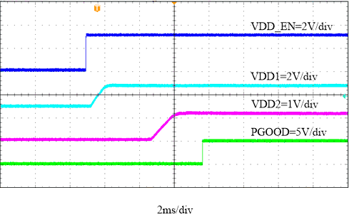 Figure 8-14 Start-Up Through VDD_EN, IVDD1OUT = 0 A, IVDD2OUT = 0
A
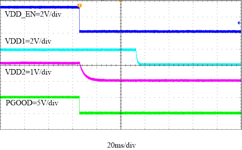 Figure 8-16 Shutdown Through VDD_EN, IVDD1OUT = 0 A, IVDD2OUT = 0
A
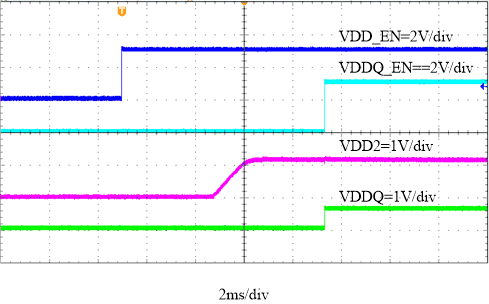
| IVDD2OUT = 0 A |
IVDDQ
= 0 A |
|
Figure 8-18 VDDQ
Start-Up Through VDDQ_EN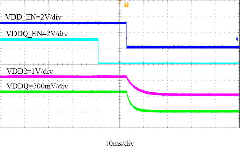
| IVDD2OUT = 0 A |
IVDDQ
= 0 A |
|
Figure 8-20 VDDQ
Shutdown Through VDDQ_EN
| IVDD2OUT = 0 A |
IVDDQ
= 0 A |
|
Figure 8-22 VDDQ
Start-Up Through VDD_EN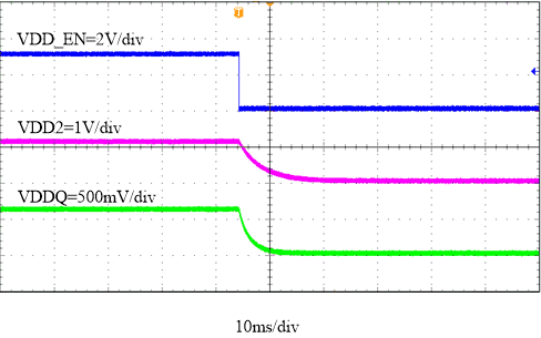
| IVDD2OUT = 0 A |
IVDDQ
= 0 A |
|
Figure 8-24 VDDQ
Shutdown Through VDD_EN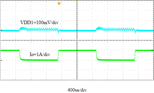 Figure 8-26 VDD1
Transient Response, 0 A to 1 A
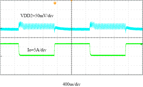 Figure 8-28 VDD2
Transient Response, 0.1 A to 6.4 A
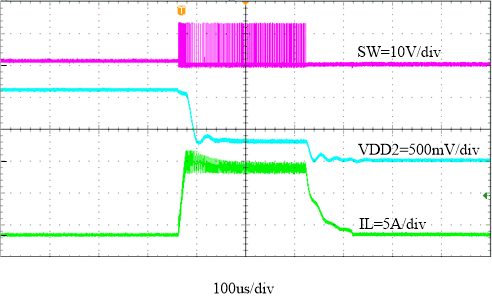 Figure 8-30 VDD2
Normal Operation to Output Hard Short
 Figure 8-3 VDD2
Efficiency Curve, VOUT = 1.1 V
 Figure 8-5 VDD2
Load Regulation, VOUT = 1.1 V
 Figure 8-7 VDDQ
Load Regulation, VOUT = 0.6 V
 Figure 8-9 VDD1 Line Regulation,
VOUT = 1.8 V
 Figure 8-11 VDD1 Output Voltage
Ripple, IOUT = 0 A
 Figure 8-13 VDD1 Output Voltage
Ripple, IOUT = 1 A
 Figure 8-15 Start-Up Through VDD_EN, IVDD1OUT = 1 A, IVDD2OUT = 8
A
 Figure 8-17 Shutdown Through VDD_EN, IVDD1OUT = 1 A, IVDD2OUT = 8
A


 Figure 8-29 VDD1
Normal Operation to Output Hard Short
 Figure 8-4 VDD1
Efficiency Curve, VOUT = 1.8 V
 Figure 8-6 VDD1
Load Regulation, VOUT = 1.8 V
 Figure 8-8 VDD2 Line
Regulation,VOUT = 1.1 V
 Figure 8-10 VDD2 Output Voltage
Ripple, IOUT = 0 A
 Figure 8-12 VDD2 Output Voltage
Ripple, IOUT = 8 A
 Figure 8-14 Start-Up Through VDD_EN, IVDD1OUT = 0 A, IVDD2OUT = 0
A
 Figure 8-16 Shutdown Through VDD_EN, IVDD1OUT = 0 A, IVDD2OUT = 0
A


 Figure 8-30 VDD2
Normal Operation to Output Hard Short