JAJSNJ1H May 2013 – December 2021 TPS65310A-Q1
PRODUCTION DATA
- 1 特長
- 2 アプリケーション
- 3 概要
- 4 Revision History
- 5 概要 (続き)
- 6 Pin Configuration and Functions
- 7 Specifications
-
8 Detailed Description
- 8.1 Overview
- 8.2 Functional Block Diagram
- 8.3 Feature Description
- 8.4
Device Functional Modes
- 8.4.1 RESET
- 8.4.2 Soft Start
- 8.4.3 INIT
- 8.4.4 TESTSTART
- 8.4.5 TESTSTOP
- 8.4.6 VTCHECK
- 8.4.7 RAMP
- 8.4.8 Power-Up Sequencing
- 8.4.9 Power-Down Sequencing
- 8.4.10 Active
- 8.4.11 ERROR
- 8.4.12 LOCKED
- 8.4.13 LPM0
- 8.4.14 Shutdown
- 8.4.15 Wake Pin
- 8.4.16 IRQ Pin
- 8.4.17 VBAT Undervoltage Warning
- 8.4.18 VIN Over Or Undervoltage Protection
- 8.4.19 External Protection
- 8.4.20 Overtemperature Detection And Shutdown
- 8.4.21 Independent Voltage Monitoring
- 8.4.22 GND Loss Detection
- 8.4.23 Reference Voltage
- 8.4.24 Shutdown Comparator
- 8.4.25 LED And High-Side Switch Control
- 8.4.26 Window Watchdog
- 8.4.27 Timeout In Start-Up Modes
- 8.5 Programming
- 8.6 Register Maps
-
9 Application and Implementation
- 9.1 Application Information
- 9.2
Typical Applications
- 9.2.1 Buck Controller 1
- 9.2.2 Synchronous Buck Converters BUCK2 and BUCK3
- 9.2.3 BOOST Converter
- 9.2.4 Linear Regulator
- 10Power Supply Recommendations
- 11Layout
- 12Device and Documentation Support
- 13Mechanical, Packaging, and Orderable Information
パッケージ・オプション
メカニカル・データ(パッケージ|ピン)
- RVJ|56
サーマルパッド・メカニカル・データ
- RVJ|56
発注情報
8.4.15 Wake Pin
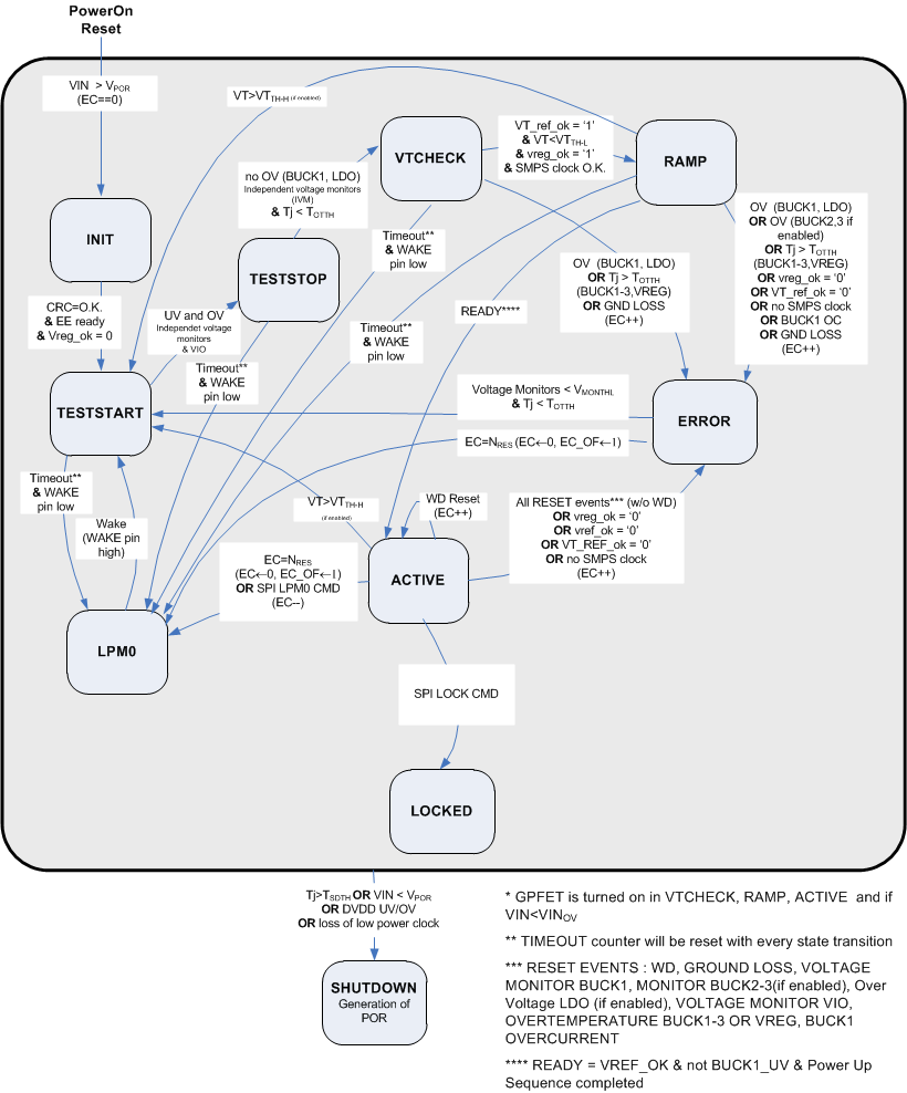
Only when the device is in LPM0 mode, it can be activated by a positive voltage on the WAKE pin with a minimum pulse width tWAKE. A valid wake condition is latched. Normal deactivation of the device can only occur through the SPI Interface by sending an SPI command to enter LMP0. Once in LMP0, the device stays in LPM0 when the WAKE pin is low, or restarts to TESTSTART when the WAKE pin is high.
The WAKE pin has an internal pulldown resistance RPD-WAKE, and the voltage on the pin is not allowed to exceed 60 V. A higher voltage compliance level in the application can be achieved by applying an external series resistor between the WAKE pin and the external wake-up signal.
The device cannot be re-enabled by toggling the WAKE pin when the device is in LOCKED state (by SPI command).
 Figure 8-5 Operating Mode Transitions