JAJSIR5C October 2019 – October 2023 TPS65313-Q1
PRODUCTION DATA
- 1
- 1 特長
- 2 アプリケーション
- 3 概要
- 4 デバイスの機能ブロック図
- 5 Revision History
- 6 概要 (続き)
- 7 Device Option Table
- 8 Pin Configuration and Functions
-
9 Specifications
- 9.1 Absolute Maximum Ratings
- 9.2 ESD Ratings
- 9.3 Recommended Operating Conditions
- 9.4 Thermal Information
- 9.5 Power-On-Reset, Current Consumption, and State Timeout Characteristics
- 9.6 PLL/Oscillator and SYNC_IN Pin Characteristics
- 9.7 Wide-VIN Synchronous Buck Regulator (Wide-VIN BUCK) Characteristics
- 9.8 Low-Voltage Synchronous Buck Regulator (LV BUCK) Characteristics
- 9.9 Synchronous Boost Converter (BOOST) Characteristics
- 9.10 Internal Voltage Regulator (VREG) Characteristics
- 9.11 Voltage Monitors for Regulators Characteristics
- 9.12 External General Purpose Voltage Monitor Characteristics
- 9.13 VIN and VIN_SAFE Under-Voltage and Over-Voltage Warning Characteristics
- 9.14 WAKE Input Characteristics
- 9.15 NRES (nRESET) Output Characteristics
- 9.16 ENDRV/nIRQ Output Characteristics
- 9.17 Analog DIAG_OUT
- 9.18 Digital INPUT/OUTPUT IOs (SPI Interface IOs, DIAG_OUT/SYNC_OUT, MCU_ERROR)
- 9.19 BUCK1, BUCK2, BOOST Thermal Shutdown / Over Temperature Protection Characteristics
- 9.20 PGNDx Loss Detection Characteristics
- 9.21 SPI Timing Requirements
- 9.22 SPI Characteristics
- 9.23 Typical Characteristics
- 10Parameter Measurement Information
-
11Detailed Description
- 11.1 Overview
- 11.2 Functional Block Diagram
- 11.3
Wide-VIN Buck Regulator (BUCK1)
- 11.3.1 Fixed-Frequency Voltage-Mode Step-Down Regulator
- 11.3.2 Operation
- 11.3.3 Voltage Monitoring (Monitoring and Protection)
- 11.3.4 Overcurrent Protection (Monitoring and Protection)
- 11.3.5 Thermal Warning and Shutdown Protection (Monitoring and Protection)
- 11.3.6 Overvoltage Protection (OVP) (Monitoring and Protection)
- 11.3.7 Extreme Overvoltage Protection (EOVP) (Monitoring and Protection)
- 11.4
Low-Voltage Buck Regulator (BUCK2)
- 11.4.1 Fixed-Frequency Peak-Current Mode Step-Down Regulator
- 11.4.2 Operation
- 11.4.3 Output Voltage Monitoring (Monitoring and Protection)
- 11.4.4 Overcurrent Protection (Monitoring and Protection)
- 11.4.5 Thermal Sensor Warning and Thermal Shutdown Protection (Monitoring and Protection)
- 11.4.6 Overvoltage Protection (OVP) (Monitoring and Protection)
- 11.5 Low-Voltage Boost Converter (BOOST)
- 11.6 VREG Regulator
- 11.7
BUCK1, BUCK2, and BOOST Switching Clocks and Synchronization (SYNC_IN) Clock
- 11.7.1 Internal fSW Clock Configuration (fSW Derived from an Internal Oscillator)
- 11.7.2 BUCK1 Switching Clock-Monitor Error (Internal fSW Clock Configuration)
- 11.7.3 BUCK2 Switching Clock-Monitor Error (Internal fSW Clock Configuration)
- 11.7.4 BOOST Switching Clock-Monitor Error (Internal fSW Clock Configuration)
- 11.7.5 External fSW Clock Configuration (fSW Derived from SYNC_IN and PLL Clocks)
- 11.8 BUCK1, BUCK2, and BOOST Switching-Clock Spread-Spectrum Modulation
- 11.9
Monitoring, Protection and Diagnostics Overview
- 11.9.1 Safety Functions and Diagnostic Overview
- 11.9.2 Supply Voltage Monitor (VMON)
- 11.9.3 Clock Monitors
- 11.9.4 Analog Built-In Self-Test
- 11.9.5 Logic Built-In Self-Test
- 11.9.6 Junction Temperature Monitors
- 11.9.7 Current Limit
- 11.9.8 Loss of Ground (GND)
- 11.9.9 Diagnostic Output Pin (DIAG_OUT)
- 11.9.10 Watchdog
- 11.9.11 MCU Error Signal Monitor
- 11.9.12 NRES Driver
- 11.9.13 ENDRV/nIRQ Driver
- 11.9.14 CRC Protection for the Device Configuration Registers
- 11.9.15 CRC Protection for the Device EEPROM Registers
- 11.10 General-Purpose External Supply Voltage Monitors
- 11.11 Analog Wake-up and Failure Latch
- 11.12 Power-Up and Power-Down Sequences
- 11.13 Device Fail-Safe State Controller (Monitoring and Protection)
- 11.14 Wakeup
- 11.15 Serial Peripheral Interface (SPI)
- 11.16 Register Maps
-
12Applications, Implementation, and Layout
- 12.1 Application Information
- 12.2
Typical Application
- 12.2.1 Design Requirements
- 12.2.2
Detailed Design Procedure
- 12.2.2.1 Selecting the BUCK1, BUCK2, and BOOST Output Voltages
- 12.2.2.2 Selecting the BUCK1, BUCK2, and BOOST Inductors
- 12.2.2.3 Selecting the BUCK1 and BUCK2 Output Capacitors
- 12.2.2.4 Selecting the BOOST Output Capacitors
- 12.2.2.5 Input Filter Capacitor Selection for BUCK1, BUCK2, and BOOST
- 12.2.2.6 Input Filter Capacitors on AVIN and VIN_SAFE Pins
- 12.2.2.7 Bootstrap Capacitor Selection
- 12.2.2.8 Internal Linear Regulator (VREG) Output Capacitor Selection
- 12.2.2.9 EXTSUP Pin
- 12.2.2.10 WAKE Input Pin
- 12.2.2.11 VIO Supply Pin
- 12.2.2.12 External General-Purpose Voltage Monitor Input Pins (EXT_VSENSE1 and EXT_VSENSE2)
- 12.2.2.13 SYNC_IN Pin
- 12.2.2.14 MCU_ERR Pin
- 12.2.2.15 NRES Pin
- 12.2.2.16 ENDRV/nIRQ Pin
- 12.2.2.17 DIAG_OUT Pin
- 12.2.2.18 SPI Pins (NCS,SCK, SDI, SDO)
- 12.2.2.19 PBKGx, AGND, DGND, and PGNDx Pins
- 12.2.2.20 Calculations for Power Dissipation and Junction Temperature
- 12.2.3 Application Curves
- 12.2.4 Layout
- 12.3 Power Supply Coupling and Bulk Capacitors
- 13Device and Documentation Support
- 14Mechanical, Packaging, and Orderable Information
11.9.11 MCU Error Signal Monitor
The MCU error signal monitor (ESM) monitors the system MCU-error events signaled over the MCU_ERR input pin. The ESM is configurable for two different operating modes. The first mode is TMS570 mode, in which the ESM detects a low-pulse signal with a programmable low-pulse width duration threshold. The second mode is PWM mode, in which the ESM detects a PWM signal with a programmable minimum and maximum pulse-width threshold for the low pulse and high pulse.
The operating mode of the ESM is controlled through the MCU_ESM_CFG bit in the SAFETY_CFG3 SPI register. The ESM is disabled by default, and can be activated by setting the MCU_ESM_EN bit to 1b in the SAFETY_CHECK_CTRL SPI register.
In TMS570 mode, the SAFETY_ERR_PWM_LMAX register sets the threshold of the low-signal duration. When TMS570 mode is enabled and monitoring signal is high, monitoring starts after the first high to low signal transition. If monitoring signal is low when TMS570 mode is enabled and monitoring signal does not transition high for the duration of the tTMS570_START_TO start-up time-out window, an error is detected, the ESM failure counter (MCU_ESM_FC[3:0]) is incremented, and the tTMS570_START_TO start-up time-out window is restarted again. The duration of the start-up time-out window tTMS570_START_TO is set by the SAFETY_ERR_PWM_LMAX register and SAFETY_ERR_PWM_HMAX register setting (tPWM_LOWMAX + tPWM_HIGHMAX).
In PWM mode, the SAFETY_ERR_PWM_LMIN and SAFETY_ERR_PWM_LMAX registers set the thresholds for the minimum and maximum low-pulse durations. The SAFETY_ERR_PWM_HMIN and SAFETY_ERR_PWM_HMAX registers set the thresholds for the minimum and maximum high-pulse durations.
When the PWM mode is enabled, monitoring starts after the rising or falling edge of the signal. If no edge is detected within the time-out window (tPWM_LOWMAX + tPWM_HIGHMAX), then an error is detected and the ESM failure counter (MCU_ESM_FC[3:0]) increments. If the monitored signal duration is shorter than the tPWM_HIGHMIN or tPWM_LOWMIN time or if the monitored signal duration is longer than the tPWM_HIGHMAX or tPWM_LOWMAX time, the following occurs:
- An error is detected.
- The MCU_ESM_FC[3:0] failure counter increments.
- A new monitoring cycle starts.
Correct signaling is detected for the low signal when the low-signal duration is from the tPWM_LOWMIN time interval to the tPWM_LOWMAX time interval and is followed by a high-signal width duration from the tPWM_HIGHMIN time interval to the tPWM_HIGHMAX time interval. Correct signaling is detected for the high signal when the high-signal duration is from the tPWM_HIGHMIN time interval to the tPWM_HIGHMAX time interval and is followed by a low signal with a duration from the SAFETY_ERR_PWM_LMIN interval to the SAFETY_ERR_PWM_LMAX interval.
The MCU_ESM_FC[3:0] counter decrements when a correct signal is detected. When monitoring starts, a new monitoring event starts any time after an error is detected or when correct signaling is detected.
The MCU_ESM_FC[3:0] counter increments after an MCU signaling error is detected. If the device is in the ACTIVE state, the MCU_ESM_FC[3:0] counter is greater than the programmed threshold (MCU_ESM_FC_ENDRV_TH) and MCU_ESM_RST_EN configuration bit is set to 0b, the following occurs:
- The device goes into the SAFE state.
- The ENDRV/nIRQ pin is disabled (driven low).
- The MCU_ESM_FAIL and MCU_ESM_RST_FAIL status bits are set in the SAFETY_ERR_STAT3 register.
If the device is in the DIAGNOSTIC or ACTIVE state, the MCU_ESM_FC[3:0] counter is greater than the MCU_ESM_FC_RST_TH[3:0] threshold, and the MCU_ESM_RST_EN configuration bit is set to 1b, the device goes into the RESET state. The MCU_ESM_FAIL and MCU_ESM_RST_FAIL status bits are also set in the SAFETY_ERR_STAT3 register.
If the device is in the DIAGNOSTIC or ACTIVE state, the MCU_ESM_FC[3:0] counter is greater than the MCU_ESM_FC_RST_TH[3:0] threshold, and the MCU_ESM_RST_EN configuration bit is set to 0b, the device goes into the SAFE state. The MCU_ESM_FAIL and MCU_ESM_RST_FAIL status bits are also set in the SAFETY_ERR_STAT3 register. If the device is already in the SAFE state and if the MCU_ESM_FC_RST_TH[3:0] threshold is equal to or less than the MCU_ESM_FC_ENDRV_TH[3:0] threshold, no action occurs.
Regardless of the configuration mode of the MCU ESM, a new MCU ESM cycle starts and the MCU_ESM_FC[3:0] and MCU_ESM_FAIL status bits are initialized each time one of the following occurs:
- When a NPOR event occurs.
- When the device goes to the RESET state.
- After the LBIST run is complete.
- After the MCU_ESM_CFG bit toggles when changing the ESM configuration mode.
- After the MCU_ESM_EN bit is set to 0b.
Regardless of the configuration mode of the MCU ESM, the MCU_ESM_FC[3:0] bit is initialized to its default value each time one of the following occurs:
- When the device goes into the DIAGNOSTIC state from the SAFE state.
- When the device goes into the RESET state.
- After the LBIST run is complete.
- After the MCU_ESM_EN bit toggles from 0b to 1b.
- After the MCU_ESM_CFG bit toggles from 0b to 1b or from 1b to 0b.
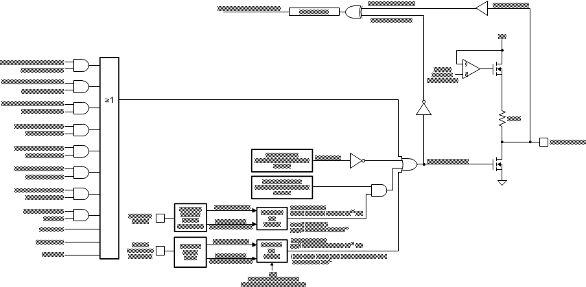 Figure 11-20 MCU Error Signaling Monitor (ESM) With MCU ESM Failure Counter and WD Failure Counter
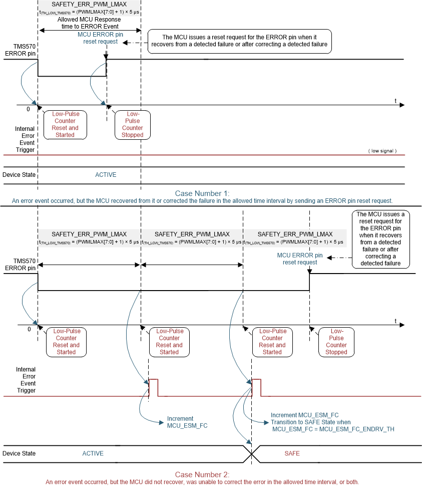 Figure 11-21 MCU ESM TMS570 Mode
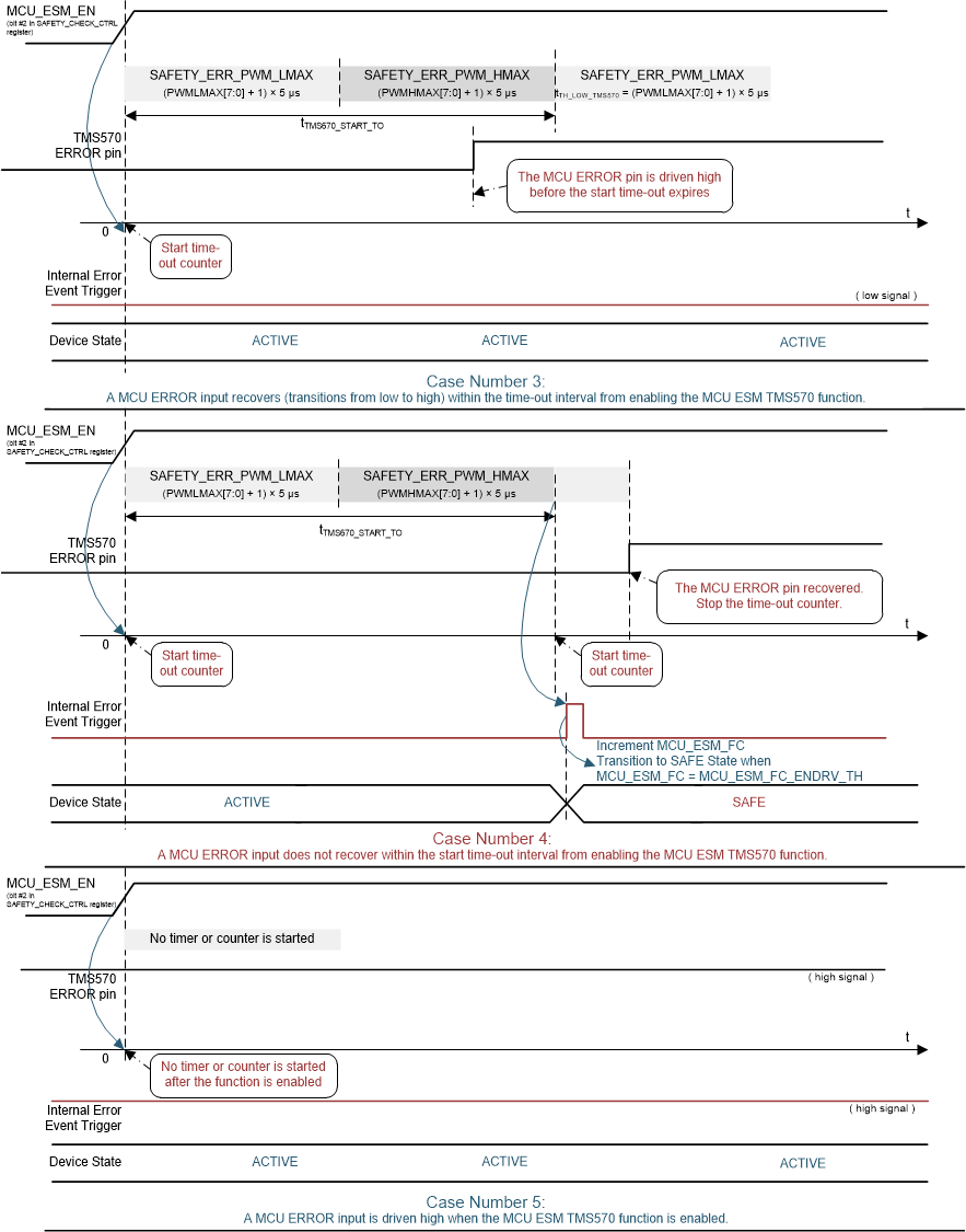 Figure 11-22 MCU ESM TMS570 Mode (Time-Out)
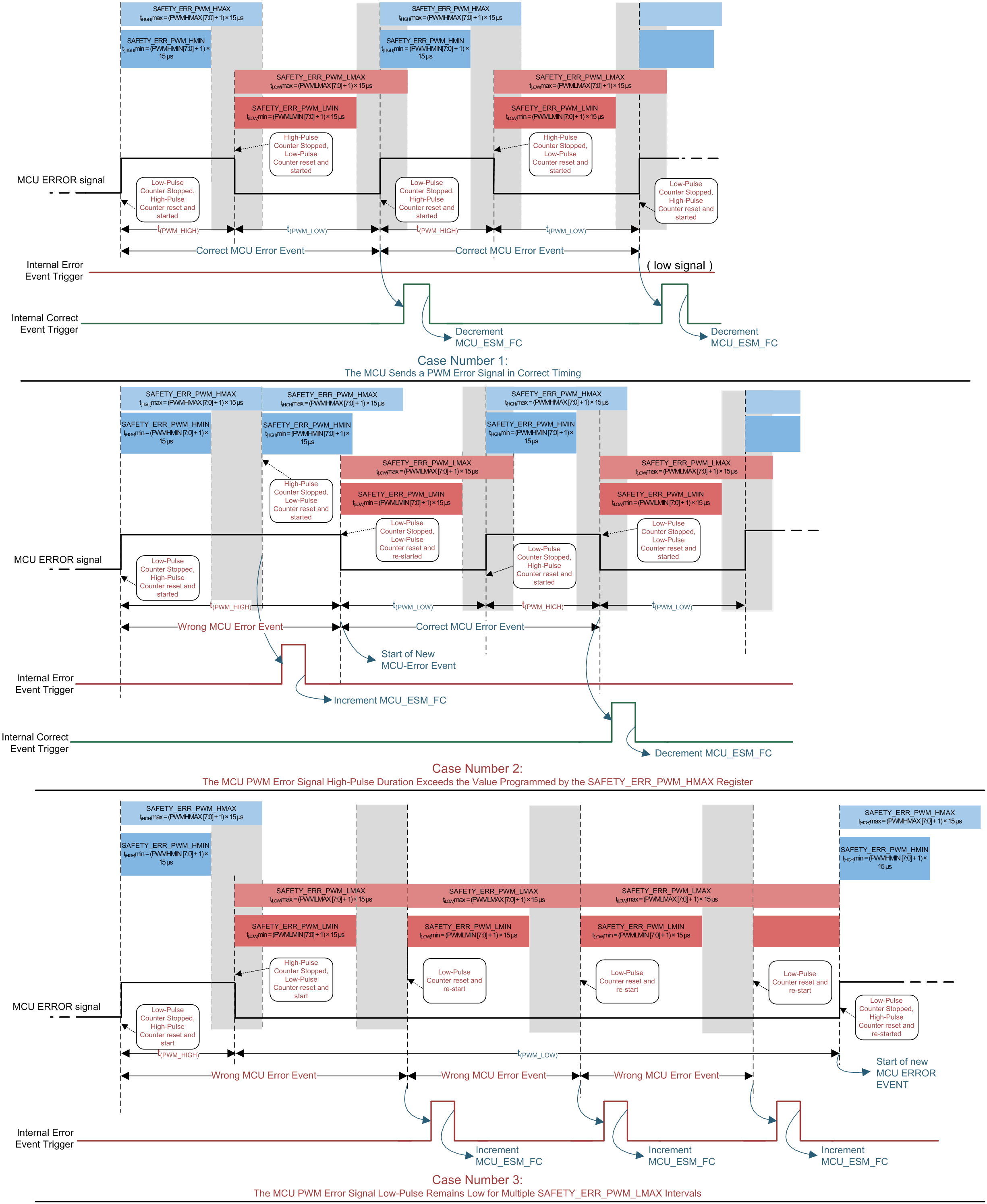 Figure 11-23 MCU ESM PWM Mode (Case Scenarios 1, 2, and 3)
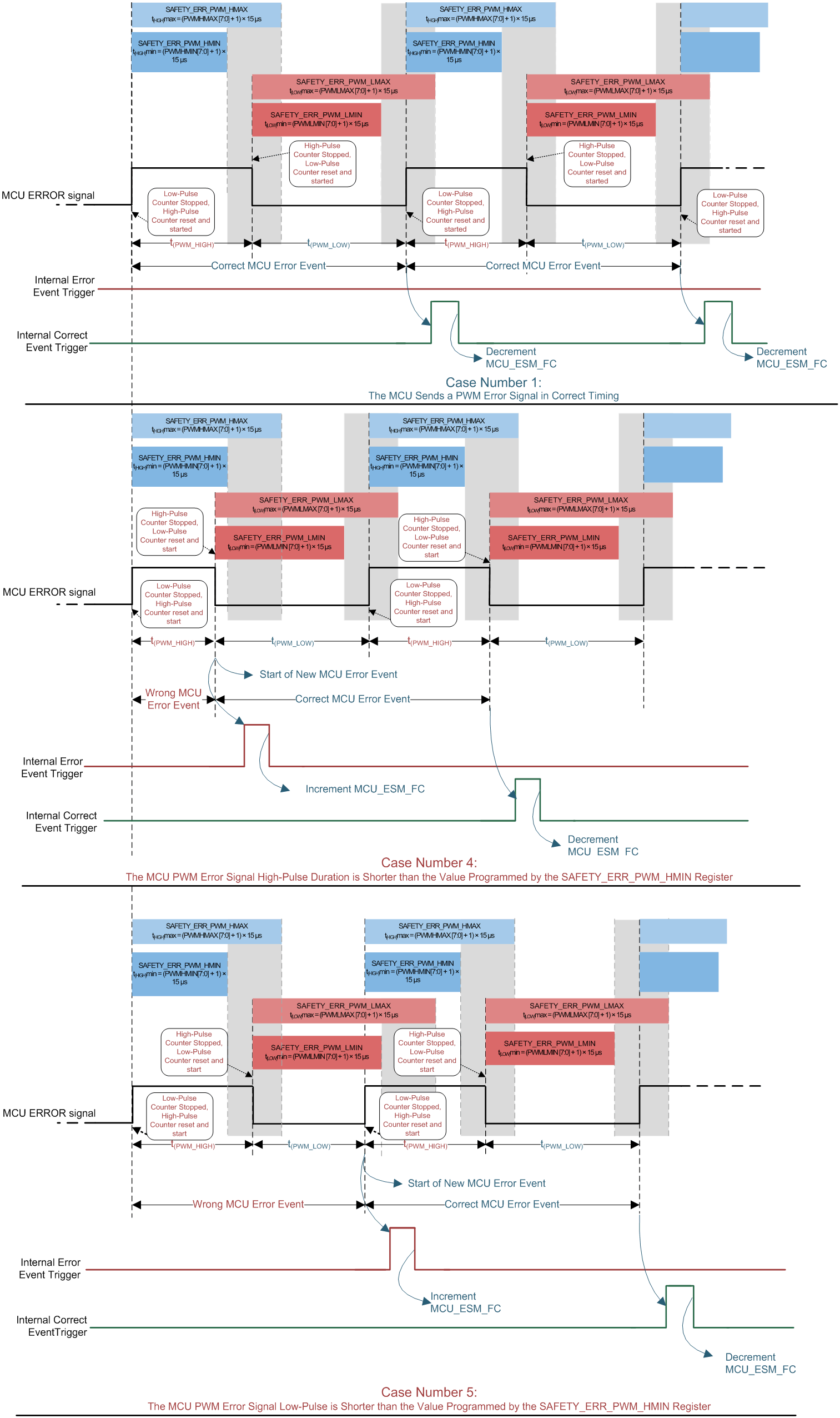 Figure 11-24 MCU ESM PWM Mode (Case Scenarios 1, 4, and 5)
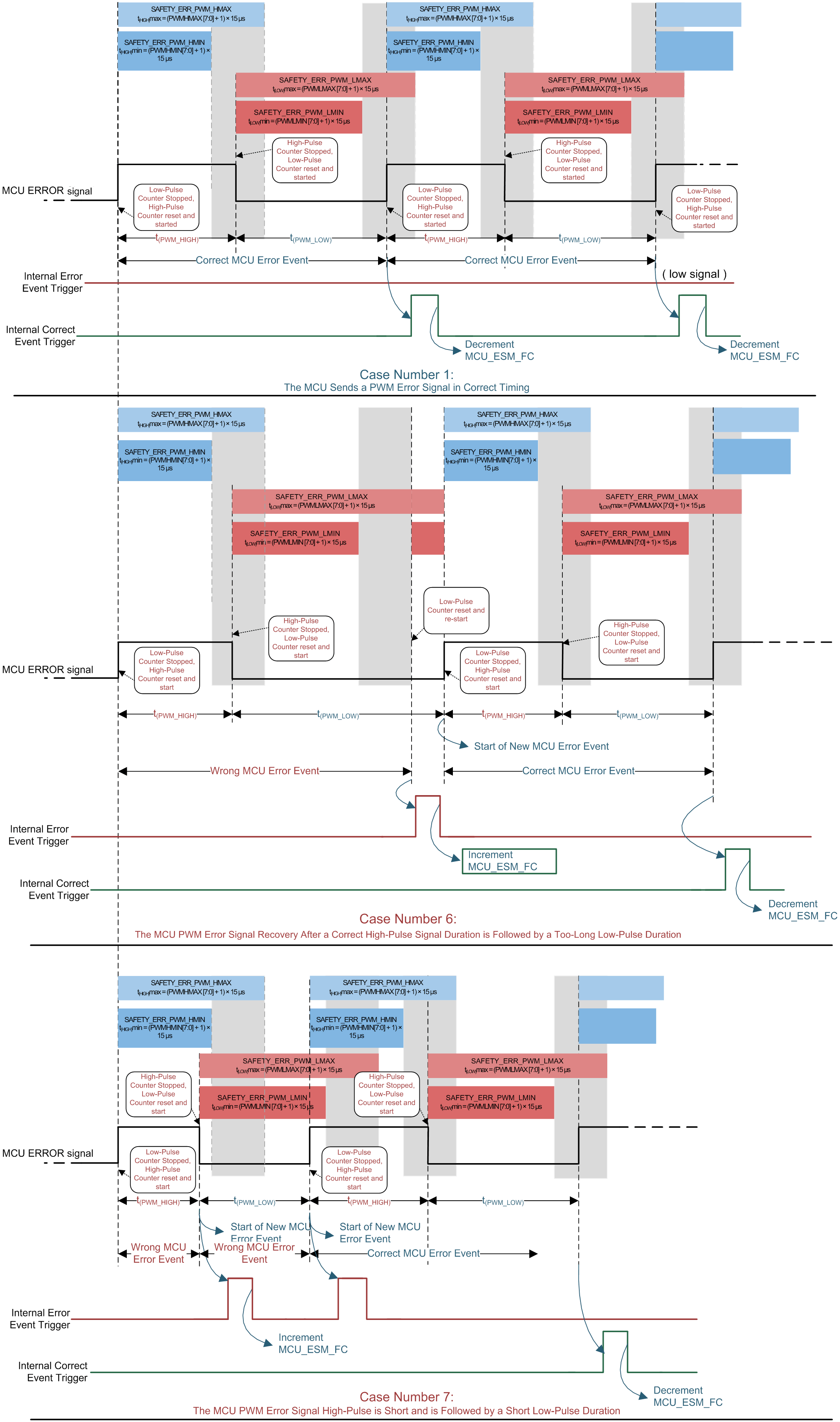 Figure 11-25 MCU ESM PWM Mode (Case Scenarios 1, 6, and 7)
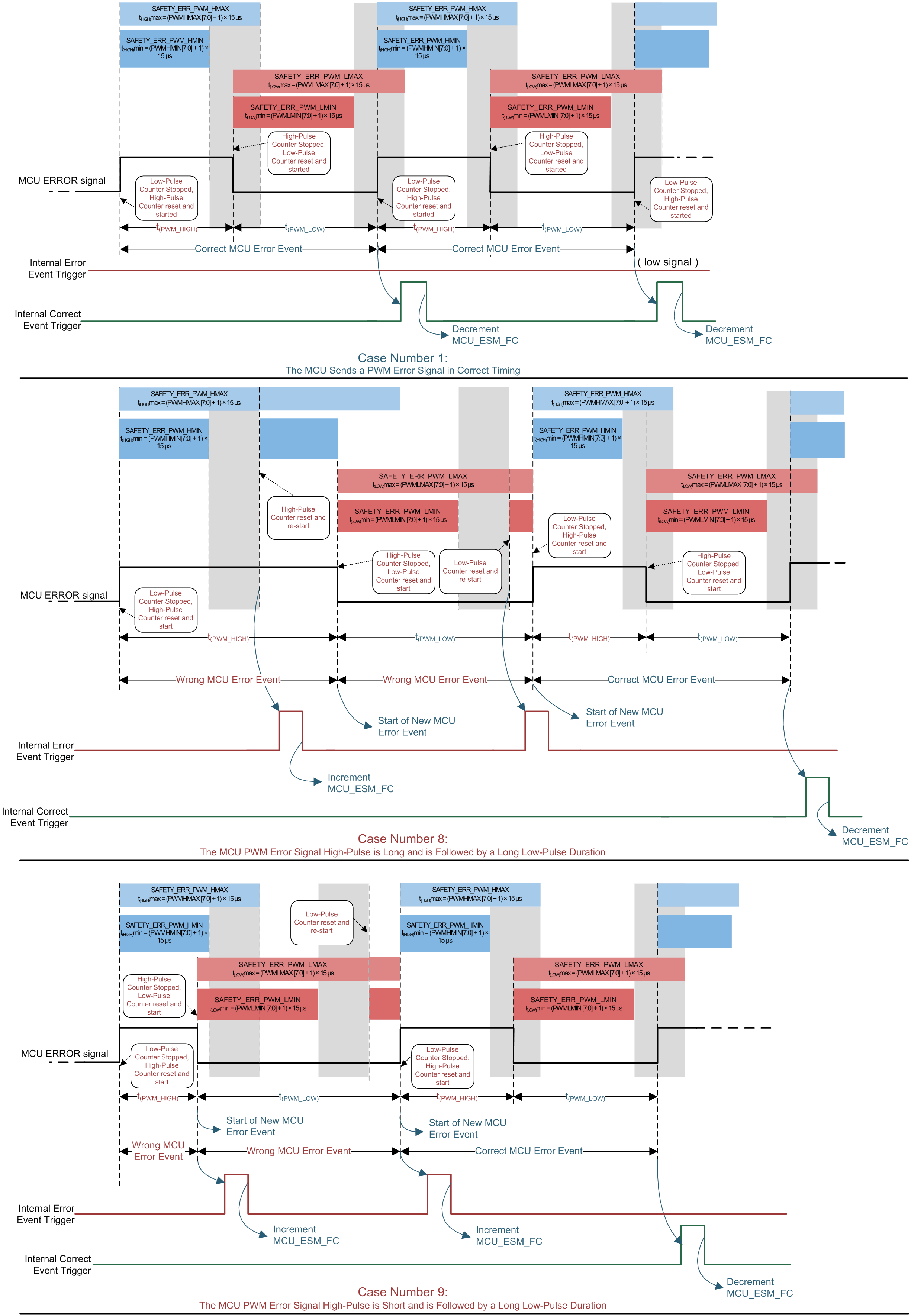 Figure 11-26 MCU ESM PWM Mode (Case Scenarios 1, 8, and 9)
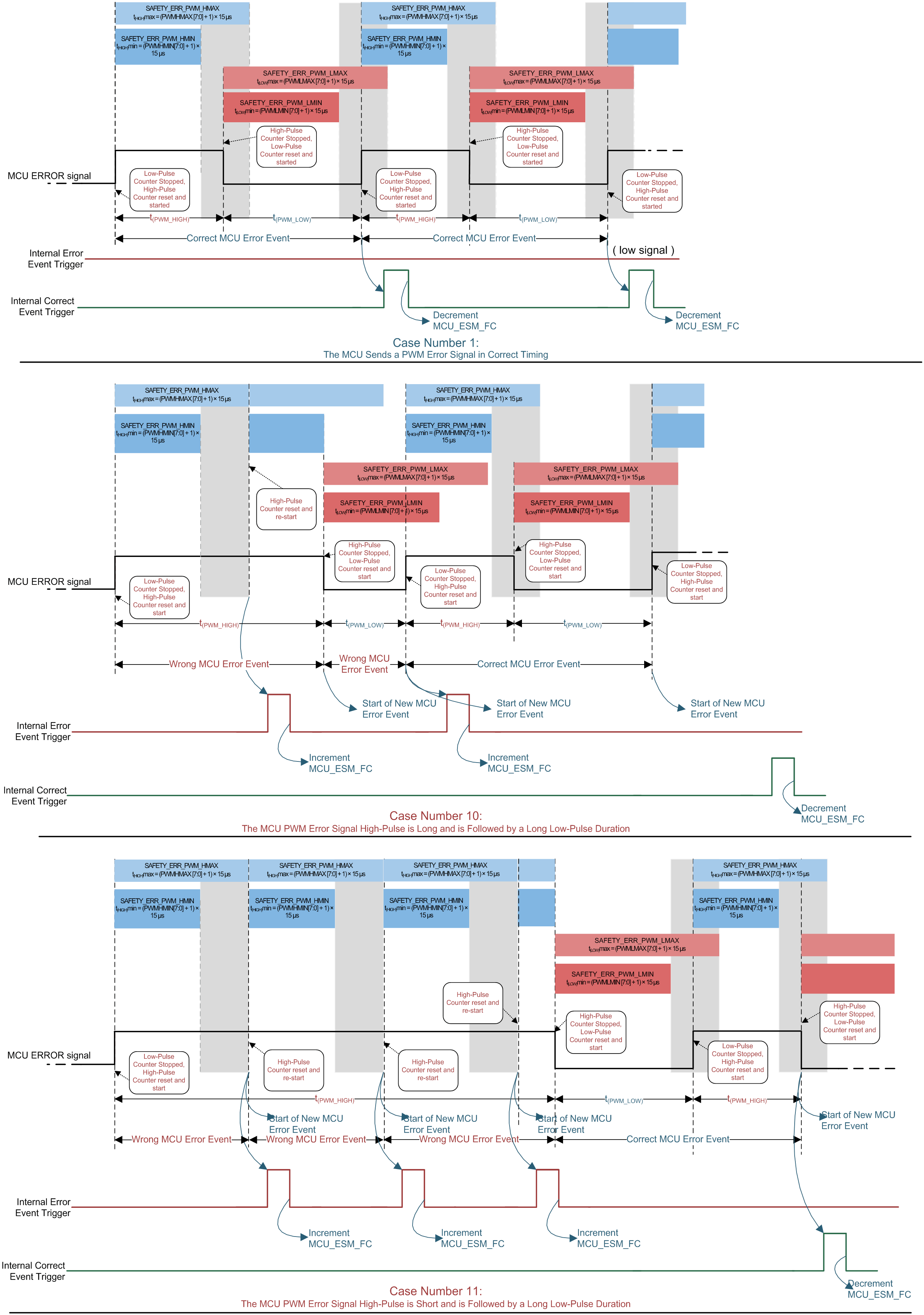 Figure 11-27 MCU ESM PWM Mode (Case Scenarios 1, 10, and 11)
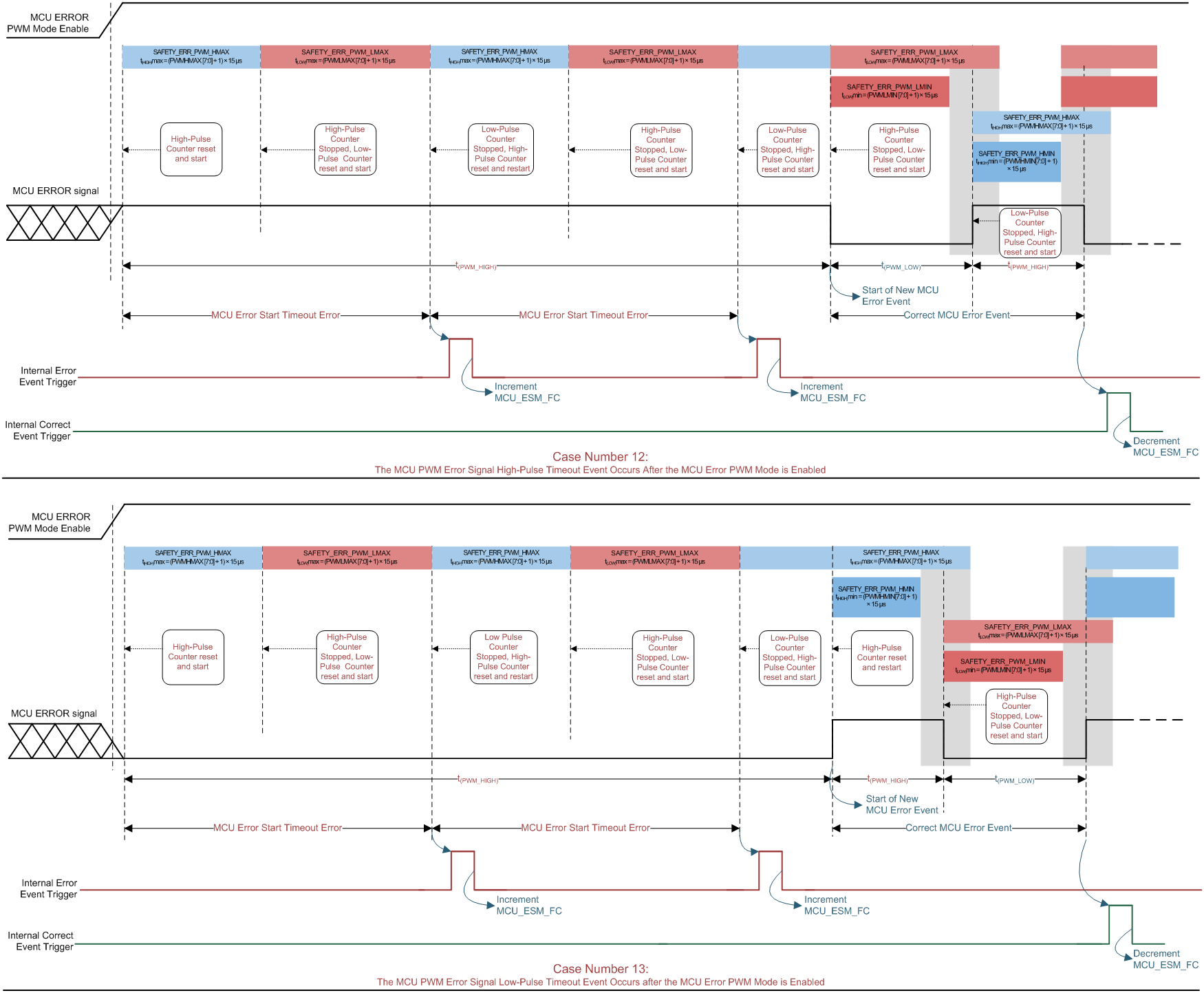 Figure 11-28 MCU ESM PWM Mode Time-Out Events After PWM Mode is Enabled
 (Case Scenarios 12 and 13)