JAJSFE5C October 2009 – May 2018 TPS65720 , TPS65721
PRODUCTION DATA.
- 1 特長
- 2 アプリケーション
- 3 概要
- 4 改訂履歴
- 5 概要(続き)
- 6 Device Options
- 7 Pin Configuration and Functions
- 8 Specifications
-
9 Detailed Description
- 9.1 Overview
- 9.2 Functional Block Diagrams
- 9.3
Feature Description
- 9.3.1 Battery Charger and Power Path
- 9.3.2 Power-Path Management
- 9.3.3 Battery Charging
- 9.3.4 Thermal Regulation and Thermal Shutdown
- 9.3.5 Battery Pack Temperature Monitoring
- 9.3.6 DCDC1 Converter
- 9.3.7 Power Save Mode
- 9.3.8 Short-Circuit Protection
- 9.3.9 Thermal Shutdown
- 9.3.10 LDO1
- 9.4 Device Functional Modes
- 9.5 Programming
- 9.6
Register Maps
- 9.6.1 CHGSTATUS Register Address: 01h (read only)
- 9.6.2 CHGCONFIG0 Register Address: 02h (read/write)
- 9.6.3 CHGCONFIG1 Register Address: 03h (read/write)
- 9.6.4 CHGCONFIG2 Register Address: 04h (read/write)
- 9.6.5 CHGCONFIG3 Register Address: 05h (read/write)
- 9.6.6 CHGSTATE Register Address: 06h (read only)
- 9.6.7 DEFDCDC1 Register Address: 07h (read/write)
- 9.6.8 LDO_CTRL Register Address: 08h (read/write)
- 9.6.9 CONTROL0 Register Address: 09h (read/write)
- 9.6.10 CONTROL1 Register Address: 0Ah (read/write)
- 9.6.11 GPIO_SSC Register Address: 0Bh (read/write)
- 9.6.12 GPIODIR Register Address: 0Ch (read/write)
- 9.6.13 IRMASK0 Register Address: 0Dh (read/write)
- 9.6.14 IRMASK1 Register Address: 0Eh (read/write)
- 9.6.15 IRMASK2 Register Address: 0Fh (read/write)
- 9.6.16 IR0 Register Address: 10h (read only)
- 9.6.17 IR1 Register Address: 11h (read)
- 9.6.18 IR2 Register Address: 12h (read)
- 10Application and Implementation
- 11Power Supply Recommendations
- 12Layout
- 13デバイスおよびドキュメントのサポート
- 14メカニカル、パッケージ、および注文情報
8.9 Typical Characteristics
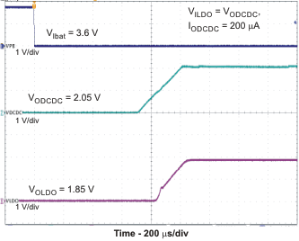
The graphs have been generated on the TPS65720YFF EVM with the inductors as mentioned in the graphs. See the TPS65720EVM User's Guide (SLVU324) for details on the layout.Table 1. Table Of Graphs
| FIGURE | |||
|---|---|---|---|
| Startup DCDC1 and LDO1 | Scope plot using TPS65720 (battery powered) for
PB_IN; Vo_DCDC1; Vo_LDO1 |
Figure 2 | |
| KISET vs RISET | Figure 3, Figure 4, Figure 5, Figure 6 | ||

![TPS65720 TPS657201 TPS657202 TPS65721 KISET vs RISET; ICH_SCL[1,0] = 01 TPS65720 TPS657201 TPS657202 TPS65721 ki2_ri_lvs979.gif](/ods/images/JAJSFE5C/ki2_ri_lvs979.gif)
![TPS65720 TPS657201 TPS657202 TPS65721 KISET vs RISET; ICH_SCL[1,0] = 11 TPS65720 TPS657201 TPS657202 TPS65721 ki4_ri_lvs979.gif](/ods/images/JAJSFE5C/ki4_ri_lvs979.gif)
![TPS65720 TPS657201 TPS657202 TPS65721 KISET vs RISET; ICH_SCL[1,0] = 00 TPS65720 TPS657201 TPS657202 TPS65721 ki_ri_lvs979.gif](/ods/images/JAJSFE5C/ki_ri_lvs979.gif)
![TPS65720 TPS657201 TPS657202 TPS65721 KISET vs RISET; ICH_SCL[1,0] = 10 TPS65720 TPS657201 TPS657202 TPS65721 ki3_ri_lvs979.gif](/ods/images/JAJSFE5C/ki3_ri_lvs979.gif)