JAJSFE5C October   2009  – May 2018 TPS65720 , TPS65721

PRODUCTION DATA.  

  1. 特長
  2. アプリケーション
  3. 概要
    1.     代表的なアプリケーションの回路図
  4. 改訂履歴
  5. 概要(続き)
  6. Device Options
  7. Pin Configuration and Functions
    1.     Pin Functions—DSBGA (TPS65720)
    2.     Pin Functions—DSBGA (TPS657201, TPS657202)
    3.     Pin Functions—WQFN (TPS65721)
  8. Specifications
    1. 8.1 Absolute Maximum Ratings
    2. 8.2 ESD Ratings
    3. 8.3 Recommended Operating Conditions
    4. 8.4 Thermal Information
    5. 8.5 Electrical Characteristics
    6. 8.6 Dissipation Ratings
    7. 8.7 Timing Requirements
    8. 8.8 Switching Characteristics
    9. 8.9 Typical Characteristics
  9. Detailed Description
    1. 9.1 Overview
    2. 9.2 Functional Block Diagrams
    3. 9.3 Feature Description
      1. 9.3.1  Battery Charger and Power Path
      2. 9.3.2  Power-Path Management
      3. 9.3.3  Battery Charging
        1. 9.3.3.1 I-PRECHARGE
        2. 9.3.3.2 ITERM
        3. 9.3.3.3 Battery Detection and Recharge
        4. 9.3.3.4 Charge Termination On/Off
        5. 9.3.3.5 Timers
        6. 9.3.3.6 Dynamic Timer Function
        7. 9.3.3.7 Charger Fault
      4. 9.3.4  Thermal Regulation and Thermal Shutdown
      5. 9.3.5  Battery Pack Temperature Monitoring
      6. 9.3.6  DCDC1 Converter
      7. 9.3.7  Power Save Mode
        1. 9.3.7.1 Dynamic Voltage Positioning
        2. 9.3.7.2 Soft Start
        3. 9.3.7.3 100% Duty Cycle Low Dropout Operation
        4. 9.3.7.4 Undervoltage Lockout
      8. 9.3.8  Short-Circuit Protection
      9. 9.3.9  Thermal Shutdown
      10. 9.3.10 LDO1
        1. 9.3.10.1 Default Voltage Setting for LDOs and DCDC1
        2. 9.3.10.2 Internal Analog Multiplexer (BAT, TS, TS_OUT); TPS657201, TPS657202 Only
        3. 9.3.10.3 Internal Battery Voltage Comparator
        4. 9.3.10.4 GPIOs, LED Drivers
        5. 9.3.10.5 RESET Output
        6. 9.3.10.6 Threshold Input (TPS65721 Only)
          1. 9.3.10.6.1 ENABLE for DCDC1 and LDO1
          2. 9.3.10.6.2 PB_IN Input
          3. 9.3.10.6.3 HOLD_DCDC1 Input
          4. 9.3.10.6.4 HOLD_LDO1 Input
          5. 9.3.10.6.5 INT Output
    4. 9.4 Device Functional Modes
      1. 9.4.1 Power Down
      2. 9.4.2 Sleep Mode
      3. 9.4.3 Standby Mode
      4. 9.4.4 Power-On Reset Mode
      5. 9.4.5 Idle Mode
    5. 9.5 Programming
      1. 9.5.1 Serial Interface
    6. 9.6 Register Maps
      1. 9.6.1  CHGSTATUS Register Address: 01h (read only)
      2. 9.6.2  CHGCONFIG0 Register Address: 02h (read/write)
      3. 9.6.3  CHGCONFIG1 Register Address: 03h (read/write)
      4. 9.6.4  CHGCONFIG2 Register Address: 04h (read/write)
      5. 9.6.5  CHGCONFIG3 Register Address: 05h (read/write)
      6. 9.6.6  CHGSTATE Register Address: 06h (read only)
      7. 9.6.7  DEFDCDC1 Register Address: 07h (read/write)
      8. 9.6.8  LDO_CTRL Register Address: 08h (read/write)
      9. 9.6.9  CONTROL0 Register Address: 09h (read/write)
      10. 9.6.10 CONTROL1 Register Address: 0Ah (read/write)
      11. 9.6.11 GPIO_SSC Register Address: 0Bh (read/write)
      12. 9.6.12 GPIODIR Register Address: 0Ch (read/write)
      13. 9.6.13 IRMASK0 Register Address: 0Dh (read/write)
      14. 9.6.14 IRMASK1 Register Address: 0Eh (read/write)
      15. 9.6.15 IRMASK2 Register Address: 0Fh (read/write)
      16. 9.6.16 IR0 Register Address: 10h (read only)
      17. 9.6.17 IR1 Register Address: 11h (read)
      18. 9.6.18 IR2 Register Address: 12h (read)
  10. 10Application and Implementation
    1. 10.1 Application Information
    2. 10.2 Typical Application
      1. 10.2.1 Design Requirements
      2. 10.2.2 Detailed Design Procedure
        1. 10.2.2.1 Output Voltage Setting
          1. 10.2.2.1.1 DCDC1
          2. 10.2.2.1.2 LDO1
        2. 10.2.2.2 Output Filter Design (Inductor and Output Capacitor)
          1. 10.2.2.2.1 Inductor Selection
          2. 10.2.2.2.2 Output Capacitor Selection
          3. 10.2.2.2.3 Input Capacitor Selection
        3. 10.2.2.3 Charger/Power Path
          1. 10.2.2.3.1 Charger Stability
          2. 10.2.2.3.2 Setting the Charge Current
          3. 10.2.2.3.3 Dynamic Power Path Management (DPPM)
      3. 10.2.3 Application Curves
  11. 11Power Supply Recommendations
  12. 12Layout
    1. 12.1 Layout Guidelines
    2. 12.2 Layout Example
  13. 13デバイスおよびドキュメントのサポート
    1. 13.1 デバイス・サポート
      1. 13.1.1 デベロッパー・ネットワークの製品に関する免責事項
    2. 13.2 ドキュメントのサポート
      1. 13.2.1 関連資料
    3. 13.3 関連リンク
    4. 13.4 ドキュメントの更新通知を受け取る方法
    5. 13.5 コミュニティ・リソース
    6. 13.6 商標
    7. 13.7 静電気放電に関する注意事項
    8. 13.8 Glossary
  14. 14メカニカル、パッケージ、および注文情報

パッケージ・オプション

メカニカル・データ(パッケージ|ピン)
サーマルパッド・メカニカル・データ
発注情報

PB_IN Input

Enables DCDC1 and LDO1 if pulled to GND. Disables DCDC1 and LDO1 if pulled high. There is no internal pull-up resistor, so a resistor is needed externally to SYS. SYS is preferred over BAT because it is powered by either AC or BAT (whichever is higher). If BAT is used, the device may not get a valid HIGH signal if the battery is deeply discharged even when there is voltage at AC.

The input signal is debounced internally by 50 ms. When PB_IN is pulled low, the DCDC1 converter and LDO1 will power up simultaneously. When PB_IN is deasserted, both converters are turned off. To leave the converters on, the HOLD_DCDC1 and HOLD_LDO1 pin need to be asserted high. The HOLD register Bit <CONTROL1:B5> will keep both, DCDC1 and LDO1 enabled if set to 1. For proper operation the PB_IN, HOLD_DCDC1 and HOLD_LDO1 pins must be terminated and must not be left floating.
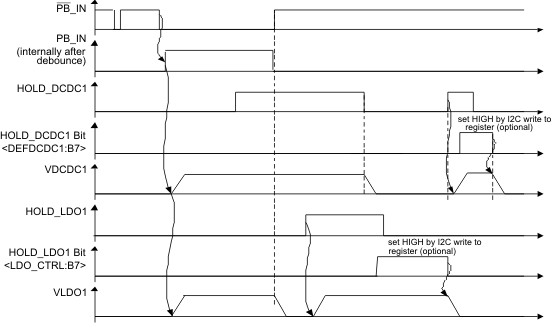
TPS65720 TPS657201 TPS657202 TPS65721 pbin_tim_lvs979.gifFigure 17. PB_IN Timing