JAJSEF7G December 2014 – February 2019 TPS659037
PRODUCTION DATA.
- 1 デバイスの概要
- 2 改訂履歴
- 3 Pin Configuration and Functions
-
4 Specifications
- 4.1 Absolute Maximum Ratings
- 4.2 ESD Ratings
- 4.3 Recommended Operating Conditions
- 4.4 Thermal Information
- 4.5 Electrical Characteristics: Latch Up Rating
- 4.6 Electrical Characteristics: LDO Regulator
- 4.7 Electrical Characteristics: Dual-Phase (SMPS12 and SMPS45) and Triple-Phase (SMPS123 and SMPS457) Regulators
- 4.8 Electrical Characteristics: Stand-Alone Regulators (SMPS3, SMPS6, SMPS7, SMPS8, and SMPS9)
- 4.9 Electrical Characteristics: Reference Generator (Bandgap)
- 4.10 Electrical Characteristics: 16-MHz Crystal Oscillator, 32-kHz RC Oscillator, and Output Buffers
- 4.11 Electrical Characteristics: DC-DC Clock Sync
- 4.12 Electrical Characteristics: 12-Bit Sigma-Delta ADC
- 4.13 Electrical Characteristics: Thermal Monitoring and Shutdown
- 4.14 Electrical Characteristics: System Control Threshold
- 4.15 Electrical Characteristics: Current Consumption
- 4.16 Electrical Characteristics: Digital Input Signal Parameters
- 4.17 Electrical Characteristics: Digital Output Signal Parameters
- 4.18 Electrical Characteristics: I/O Pullup and Pulldown
- 4.19 I2C Interface Timing Requirements
- 4.20 SPI Timing Requirements
- 4.21 Typical Characteristics
-
5 Detailed Description
- 5.1 Overview
- 5.2 Functional Block Diagram
- 5.3
Feature Description
- 5.3.1 Power Management
- 5.3.2
Power Resources (Step-Down and Step-Up SMPS Regulators, LDOs)
- 5.3.2.1
Step-Down Regulators
- 5.3.2.1.1 Sync Clock Functionality
- 5.3.2.1.2 Output Voltage and Mode Selection
- 5.3.2.1.3 Current Monitoring and Short Circuit Detection
- 5.3.2.1.4 POWERGOOD
- 5.3.2.1.5 DVS-Capable Regulators
- 5.3.2.1.6 Non DVS-Capable Regulators
- 5.3.2.1.7 Step-Down Converters SMPS12 and SMPS123
- 5.3.2.1.8 Step-Down Converter SMPS45 and SMPS457
- 5.3.2.1.9 Step-Down Converters SMPS3, SMPS6, SMPS7, SMPS8, and SMPS9
- 5.3.2.2 LDOs – Low Dropout Regulators
- 5.3.2.1
Step-Down Regulators
- 5.3.3 Long-Press Key Detection
- 5.3.4 RTC
- 5.3.5 GPADC – 12-Bit Sigma-Delta ADC
- 5.3.6 General-Purpose I/Os (GPIO Pins)
- 5.3.7 Thermal Monitoring
- 5.3.8 Interrupts
- 5.3.9 Control Interfaces
- 5.3.10 Device Identification
- 5.4 Device Functional Modes
-
6 Application and Implementation
- 6.1 Application Information
- 6.2
Typical Application
- 6.2.1 Design Requirements
- 6.2.2 Detailed Design Procedure
- 6.2.3 Application Curves
- 7 Power Supply Recommendations
- 8 Layout
- 9 デバイスおよびドキュメントのサポート
- 10メカニカル、パッケージ、および注文情報
4.20 SPI Timing Requirements
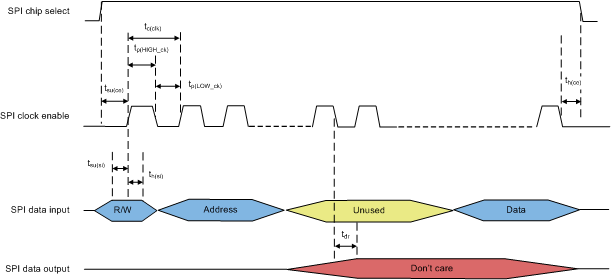
For the SPI timing diagram, see Figure 4-3| MIN | MAX | UNIT | ||
|---|---|---|---|---|
| tsu(ce) | Chip-select setup time | 30 | ns | |
| th(ce) | Chip-select hold time | 30 | ns | |
| tc(clk) | Clock cycle time | 67 | 100 | ns |
| tp(HIGH_ck) | Clock high typical pulse duration | 20 | ns | |
| tp(LOW_ck) | Clock low typical pulse duration | 20 | ns | |
| tsu(si) | Input data set up time, before clock active edge | 5 | ns | |
| th(si) | Input data hold time, after clock active edge | 5 | ns | |
| tdr | Data retention time | 15 | ns | |
| t(CE) | Time from CE going low to CE going high | 67 | ns | |
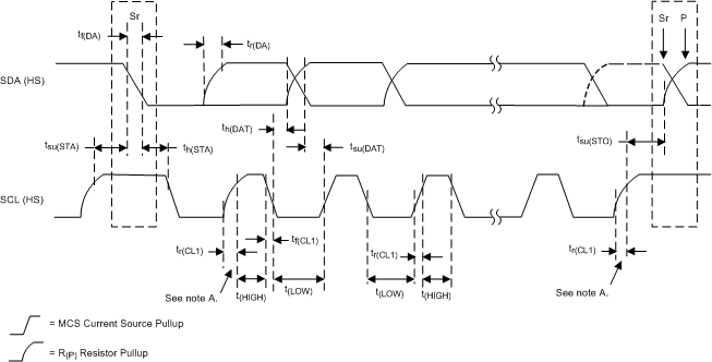
 Figure 4-1 Serial Interface Timing Diagram for F/S Mode
A. The first rising edge of the SCL (HS) signal after the repeated START condition (Sr) and after each acknowledge bit.
Figure 4-2 Serial Interface Timing Diagram For HS Mode  Figure 4-3 SPI Timing Diagram