JAJSEF7G December 2014 – February 2019 TPS659037
PRODUCTION DATA.
- 1 デバイスの概要
- 2 改訂履歴
- 3 Pin Configuration and Functions
-
4 Specifications
- 4.1 Absolute Maximum Ratings
- 4.2 ESD Ratings
- 4.3 Recommended Operating Conditions
- 4.4 Thermal Information
- 4.5 Electrical Characteristics: Latch Up Rating
- 4.6 Electrical Characteristics: LDO Regulator
- 4.7 Electrical Characteristics: Dual-Phase (SMPS12 and SMPS45) and Triple-Phase (SMPS123 and SMPS457) Regulators
- 4.8 Electrical Characteristics: Stand-Alone Regulators (SMPS3, SMPS6, SMPS7, SMPS8, and SMPS9)
- 4.9 Electrical Characteristics: Reference Generator (Bandgap)
- 4.10 Electrical Characteristics: 16-MHz Crystal Oscillator, 32-kHz RC Oscillator, and Output Buffers
- 4.11 Electrical Characteristics: DC-DC Clock Sync
- 4.12 Electrical Characteristics: 12-Bit Sigma-Delta ADC
- 4.13 Electrical Characteristics: Thermal Monitoring and Shutdown
- 4.14 Electrical Characteristics: System Control Threshold
- 4.15 Electrical Characteristics: Current Consumption
- 4.16 Electrical Characteristics: Digital Input Signal Parameters
- 4.17 Electrical Characteristics: Digital Output Signal Parameters
- 4.18 Electrical Characteristics: I/O Pullup and Pulldown
- 4.19 I2C Interface Timing Requirements
- 4.20 SPI Timing Requirements
- 4.21 Typical Characteristics
-
5 Detailed Description
- 5.1 Overview
- 5.2 Functional Block Diagram
- 5.3
Feature Description
- 5.3.1 Power Management
- 5.3.2
Power Resources (Step-Down and Step-Up SMPS Regulators, LDOs)
- 5.3.2.1
Step-Down Regulators
- 5.3.2.1.1 Sync Clock Functionality
- 5.3.2.1.2 Output Voltage and Mode Selection
- 5.3.2.1.3 Current Monitoring and Short Circuit Detection
- 5.3.2.1.4 POWERGOOD
- 5.3.2.1.5 DVS-Capable Regulators
- 5.3.2.1.6 Non DVS-Capable Regulators
- 5.3.2.1.7 Step-Down Converters SMPS12 and SMPS123
- 5.3.2.1.8 Step-Down Converter SMPS45 and SMPS457
- 5.3.2.1.9 Step-Down Converters SMPS3, SMPS6, SMPS7, SMPS8, and SMPS9
- 5.3.2.2 LDOs – Low Dropout Regulators
- 5.3.2.1
Step-Down Regulators
- 5.3.3 Long-Press Key Detection
- 5.3.4 RTC
- 5.3.5 GPADC – 12-Bit Sigma-Delta ADC
- 5.3.6 General-Purpose I/Os (GPIO Pins)
- 5.3.7 Thermal Monitoring
- 5.3.8 Interrupts
- 5.3.9 Control Interfaces
- 5.3.10 Device Identification
- 5.4 Device Functional Modes
-
6 Application and Implementation
- 6.1 Application Information
- 6.2
Typical Application
- 6.2.1 Design Requirements
- 6.2.2 Detailed Design Procedure
- 6.2.3 Application Curves
- 7 Power Supply Recommendations
- 8 Layout
- 9 デバイスおよびドキュメントのサポート
- 10メカニカル、パッケージ、および注文情報
5.3.4.5 RTC 32-kHz Oscillator Drift Compensation
The RTC_COMP_MSB_REG and RTC_COMP_LSB_REG registers are used to compensate for any inaccuracy of the 32-kHz clock output from the 16.384-MHz crystal oscillator. To compensate for any inaccuracy, software must perform an external calibration of the oscillator frequency, calculate the drift compensation needed versus one time hour period, and load the compensation registers with the drift compensation value.
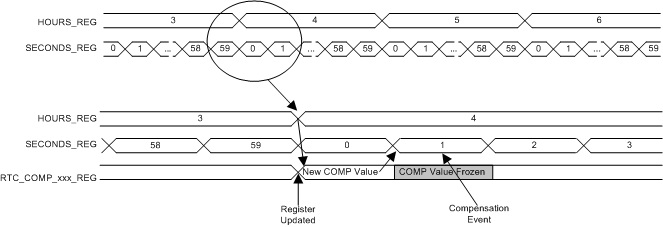
The compensation mechanism is enabled by the AUTO_COMP_EN bit in the RTC_CTRL_REG register. The process happens after the first second of each hour. The time between second 1 to second 2 (T_ADJ) is adjusted based on the settings of the two RTC_COMP_MSB_REG and RTC_COMP_LSB_REG registers. These two registers form a 16-bit, 2s complement value COMP_REG (from –32767 to 32767) that is subtracted from the 32-kHz counter as shown in Equation 3 to adjust the length of T_ADJ:

Therefore, adjusting the compensation with a 1/32768-second time unit accuracy per hour and up to 1 s per hour is possible.
Software must ensure that these registers are updated before each compensation process (there is no hardware protection). For example, software can load the compensation value into these registers after each hour event, during second 0 to second 1, just before the compensation period, happening from second 1 to second 2.
Preloading the internal 32-kHz counter with the content of the RTC_COMP_MSB_REG and
RTC_COMP_LSB_REG registers possible when setting the SET_32_COUNTER bit in the
RTC_CTRL_REG register. This setting must occur when the RTC is stopped.
Figure 5-8 shows the RTC compensation scheduling.
 Figure 5-8 RTC Compensation Scheduling