JAJSEF6L August 2013 – February 2019 TPS659038-Q1 , TPS659039-Q1
PRODUCTION DATA.
- 1 デバイスの概要
- 2 改訂履歴
- 3 Device Comparison
- 4 Pin Configuration and Functions
-
5 Specifications
- 5.1 Absolute Maximum Ratings
- 5.2 ESD Ratings
- 5.3 Recommended Operating Conditions
- 5.4 Thermal Information
- 5.5 Electrical Characteristics: Latch Up Rating
- 5.6 Electrical Characteristics: LDO Regulator
- 5.7 Electrical Characteristics: Dual-Phase (SMPS12 and SMPS45) and Triple-Phase (SMPS123 and SMPS457) Regulators
- 5.8 Electrical Characteristics: Stand-Alone Regulators (SMPS3, SMPS6, SMPS7, SMPS8, and SMPS9)
- 5.9 Electrical Characteristics: Reference Generator (Bandgap)
- 5.10 Electrical Characteristics: 16-MHz Crystal Oscillator, 32-kHz RC Oscillator, and Output Buffers
- 5.11 Electrical Characteristics: DC-DC Clock Sync
- 5.12 Electrical Characteristics: 12-Bit Sigma-Delta ADC
- 5.13 Electrical Characteristics: Thermal Monitoring and Shutdown
- 5.14 Electrical Characteristics: System Control Thresholds
- 5.15 Electrical Characteristics: Current Consumption
- 5.16 Electrical Characteristics: Digital Input Signal Parameters
- 5.17 Electrical Characteristics: Digital Output Signal Parameters
- 5.18 Electrical Characteristics: I/O Pullup and Pulldown Resistance
- 5.19 I2C Interface Timing Requirements
- 5.20 SPI Timing Requirements
- 5.21 Typical Characteristics
-
6 Detailed Description
- 6.1 Overview
- 6.2 Functional Block Diagrams
- 6.3
Feature Description
- 6.3.1 Power Management
- 6.3.2
Power Resources (Step-Down and Step-Up SMPS Regulators, LDOs)
- 6.3.2.1
Step-Down Regulators
- 6.3.2.1.1 Sync Clock Functionality
- 6.3.2.1.2 Output Voltage and Mode Selection
- 6.3.2.1.3 Current Monitoring and Short Circuit Detection
- 6.3.2.1.4 POWERGOOD
- 6.3.2.1.5 DVS-Capable Regulators
- 6.3.2.1.6 Non DVS-Capable Regulators
- 6.3.2.1.7 Step-Down Converters SMPS12 and SMPS123
- 6.3.2.1.8 Step-Down Converter SMPS45 and SMPS457
- 6.3.2.1.9 Step-Down Converters SMPS3, SMPS6, SMPS7, SMPS8, and SMPS9
- 6.3.2.2 LDOs – Low Dropout Regulators
- 6.3.2.1
Step-Down Regulators
- 6.3.3 Long-Press Key Detection
- 6.3.4 RTC
- 6.3.5 GPADC – 12-Bit Sigma-Delta ADC
- 6.3.6 General-Purpose I/Os (GPIO Terminals)
- 6.3.7 Thermal Monitoring
- 6.3.8 Interrupts
- 6.3.9 Control Interfaces
- 6.3.10 Device Identification
- 6.4 Device Functional Modes
-
7 Application and Implementation
- 7.1 Application Information
- 7.2
Typical Application
- 7.2.1 Design Requirements
- 7.2.2 Detailed Design Procedure
- 7.2.3 Application Curves
- 8 Power Supply Recommendations
- 9 Layout
- 10デバイスおよびドキュメントのサポート
- 11メカニカル、パッケージ、および注文情報
パッケージ・オプション
デバイスごとのパッケージ図は、PDF版データシートをご参照ください。
メカニカル・データ(パッケージ|ピン)
- ZWS|169
サーマルパッド・メカニカル・データ
発注情報
9.1 Layout Guidelines
As in every switch-mode-supply design, general layout rules apply:
- Use a solid ground-plane for power-ground (PGND)
- Use an independent ground for Logic, LDOs and Analog (AGND)
- Connect those Grounds at a star-point ideally underneath the IC.
- Place input capacitors as close as possible to the input-balls of the IC. This is paramount and more important than the output-loop!
- Place the inductor and output capacitor as close as possible to the phase node (or switch-node) of the IC.
- Keep the loop-area formed by Phase-node, Inductor, output-capacitor and PGND as small as possible.
- For traces and vias on power-lines, keep inductance and resistance as small as possible by using wide traces, avoid switching layers but if needed, use plenty of vias.
The goal of the previously listed guidelines is a layout that minimizes emissions, maximizes EMI-immunity, and maintains a safe operating area for the IC.
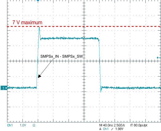
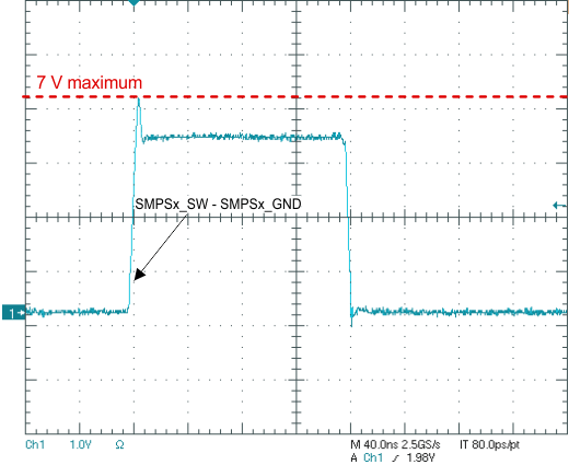
To minimize the spiking at the phase-node for both, high-side (VIN – SWx) as well as low-side (SWx – PGND), the decoupling of VIN is paramount. Appropriate decoupling and thorough layout should ensure that the spikes never exceed 7V across the high-side and low-side FETs.
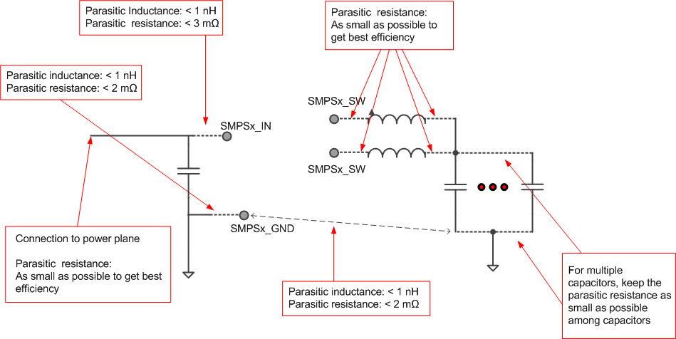
The guidelines shown in Figure 9-1 regarding parasitic inductance and resistance are recommended.
 Figure 9-1 Parasitic Inductance and Resistance
 Table 9-1 lists the maximum allowable parasitic (inductance measured at 100 MHz) and the achievable values in an optimized layout.
Table 9-1 Maximum Allowable Parasitic
| CONNECTION | MAXIMUM ALLOWABLE INDUCTANCE | MAXIMUM ALLOWABLE RESISTANCE | OPTIMIZED LAYOUT (EVM) INDUCTANCE | OPTIMIZED LAYOUT (EVM) RESISTANCE | ||
|---|---|---|---|---|---|---|
| PowerPlane – CIN | n/a | N/A for SOA, keep small for efficiency | N/A | N/A for SOA, keep small for efficiency | ||
| CIN – SMPSx_IN | 1 nH | 3 mΩ | SMPS1 | 0.533 nH | SMPS1 | 1.77 mΩ |
| SMPS2 | 0.465 nH | SMPS2 | 1.22 mΩ | |||
| SMPS3 | 0.494 nH | SMPS3 | 1.37 mΩ | |||
| SMPS4 | 0.472 nH | SMPS4 | 1.23 mΩ | |||
| SMPS5 | 0.517 nH | SMPS5 | 1.27 mΩ | |||
| SMPS6 | 0.518 nH | SMPS6 | 1.69 mΩ | |||
| SMPS7 | 0.501 nH | SMPS7 | 1.27 mΩ | |||
| SMPS8 | 0.509 nH | SMPS8 | 1.42 mΩ | |||
| SMPS9 | 0.491 nH | SMPS9 | 1.4 mΩ | |||
| CIN – SMPSx_GND | 1 nH | 2 mΩ | SMPS1 | 0.552 nH | SMPS1 | 1.21 mΩ |
| SMPS2 | 0.583 nH | SMPS2 | 0.8 mΩ | |||
| SMPS3 | 0.668 nH | SMPS3 | 0.93 mΩ | |||
| SMPS4 | 0.57 nH | SMPS4 | 0.81 mΩ | |||
| SMPS5 | 0.577 nH | SMPS5 | 0.76 mΩ | |||
| SMPS6 | 0.608 nH | SMPS6 | 1.13 mΩ | |||
| SMPS7 | 0.646 nH | SMPS7 | 0.83 mΩ | |||
| SMPS8 | 0.67 nH | SMPS8 | 0.73 mΩ | |||
| SMPS9 | 0.622 nH | SMPS9 | 0.82 mΩ | |||
| SMPSx_SW – Inductor | N/A | N/A for SOA, keep small for efficiency | N/A | SMPS1 | 1.9 mΩ | |
| SMPS2 | 0.89 mΩ | |||||
| SMPS3 | 1.99 mΩ | |||||
| SMPS4 | 0.93 mΩ | |||||
| SMPS5 | 1.37 mΩ | |||||
| SMPS6 | 1.11 mΩ | |||||
| SMPS7 | 1.17 mΩ | |||||
| SMPS8 | 1.35 mΩ | |||||
| SMPS9 | 0.88 mΩ | |||||
| Inductor – COUT | n/a | N/A for SOA, keep small for efficiency | N/A | N/A for SOA, keep small for efficiency | ||
| COUT – GND | Use dedicated GND plane to keep inductance low | mΩ | SMPS1 | 0.552 nH | SMPS1 | 1.21 mΩ |
| SMPS2 | 0.583 nH | SMPS2 | 0.8 mΩ | |||
| SMPS3 | 0.668 nH | SMPS3 | 0.93 mΩ | |||
| SMPS4 | 0.57 nH | SMPS4 | 0.81 mΩ | |||
| SMPS5 | 0.577 nH | SMPS5 | 0.76 mΩ | |||
| SMPS6 | 0.608 nH | SMPS6 | 1.13 mΩ | |||
| SMPS7 | 0.646 nH | SMPS7 | 0.83 mΩ | |||
| SMPS8 | 0.67 nH | SMPS8 | 0.73 mΩ | |||
| SMPS9 | 0.622 nH | SMPS9 | 0.82 mΩ | |||
| GND(CIN) – GND(COUT) | Use dedicated GND plane to keep inductance low | mΩ | Use dedicated GND plane to keep inductance low | mΩ | ||
Texas Instruments recommends to measure the voltages across the high-side FET (voltage at SMPSx_IN vs. SMPSx_SW) and the low-side FET (SMPSx_SW vs. SMPSx_GND) with a high-bandwidth high-sampling rate scope with a low-capacitance probe (ideally a differential probe). Measure the voltages as close as possible to the IC-balls and verify the amplitude of the spikes. A small-loop-GND-connection to the closest accessible SMPSx_GND (of the particular rail) is essential. Ideally, this measurement should be performed during start-up of the respective SMPS-rail (to take in account the inrush-current) and at high temperature.
When measuring the voltage difference between the SMPSx_IN and SMPSx_SW pins, there should be a maximum of 7 V when measuring at the pins. Similarly, when measuring the voltage difference between the SMPSx_SW and SMPSx_GND pins, there should be a maximum of 7 V when measuring at the pins.
For more information on cursor-positioning, see Figure 9-2 and Figure 9-3.

