JAJSEF6L August 2013 – February 2019 TPS659038-Q1 , TPS659039-Q1
PRODUCTION DATA.
- 1 デバイスの概要
- 2 改訂履歴
- 3 Device Comparison
- 4 Pin Configuration and Functions
-
5 Specifications
- 5.1 Absolute Maximum Ratings
- 5.2 ESD Ratings
- 5.3 Recommended Operating Conditions
- 5.4 Thermal Information
- 5.5 Electrical Characteristics: Latch Up Rating
- 5.6 Electrical Characteristics: LDO Regulator
- 5.7 Electrical Characteristics: Dual-Phase (SMPS12 and SMPS45) and Triple-Phase (SMPS123 and SMPS457) Regulators
- 5.8 Electrical Characteristics: Stand-Alone Regulators (SMPS3, SMPS6, SMPS7, SMPS8, and SMPS9)
- 5.9 Electrical Characteristics: Reference Generator (Bandgap)
- 5.10 Electrical Characteristics: 16-MHz Crystal Oscillator, 32-kHz RC Oscillator, and Output Buffers
- 5.11 Electrical Characteristics: DC-DC Clock Sync
- 5.12 Electrical Characteristics: 12-Bit Sigma-Delta ADC
- 5.13 Electrical Characteristics: Thermal Monitoring and Shutdown
- 5.14 Electrical Characteristics: System Control Thresholds
- 5.15 Electrical Characteristics: Current Consumption
- 5.16 Electrical Characteristics: Digital Input Signal Parameters
- 5.17 Electrical Characteristics: Digital Output Signal Parameters
- 5.18 Electrical Characteristics: I/O Pullup and Pulldown Resistance
- 5.19 I2C Interface Timing Requirements
- 5.20 SPI Timing Requirements
- 5.21 Typical Characteristics
-
6 Detailed Description
- 6.1 Overview
- 6.2 Functional Block Diagrams
- 6.3
Feature Description
- 6.3.1 Power Management
- 6.3.2
Power Resources (Step-Down and Step-Up SMPS Regulators, LDOs)
- 6.3.2.1
Step-Down Regulators
- 6.3.2.1.1 Sync Clock Functionality
- 6.3.2.1.2 Output Voltage and Mode Selection
- 6.3.2.1.3 Current Monitoring and Short Circuit Detection
- 6.3.2.1.4 POWERGOOD
- 6.3.2.1.5 DVS-Capable Regulators
- 6.3.2.1.6 Non DVS-Capable Regulators
- 6.3.2.1.7 Step-Down Converters SMPS12 and SMPS123
- 6.3.2.1.8 Step-Down Converter SMPS45 and SMPS457
- 6.3.2.1.9 Step-Down Converters SMPS3, SMPS6, SMPS7, SMPS8, and SMPS9
- 6.3.2.2 LDOs – Low Dropout Regulators
- 6.3.2.1
Step-Down Regulators
- 6.3.3 Long-Press Key Detection
- 6.3.4 RTC
- 6.3.5 GPADC – 12-Bit Sigma-Delta ADC
- 6.3.6 General-Purpose I/Os (GPIO Terminals)
- 6.3.7 Thermal Monitoring
- 6.3.8 Interrupts
- 6.3.9 Control Interfaces
- 6.3.10 Device Identification
- 6.4 Device Functional Modes
-
7 Application and Implementation
- 7.1 Application Information
- 7.2
Typical Application
- 7.2.1 Design Requirements
- 7.2.2 Detailed Design Procedure
- 7.2.3 Application Curves
- 8 Power Supply Recommendations
- 9 Layout
- 10デバイスおよびドキュメントのサポート
- 11メカニカル、パッケージ、および注文情報
パッケージ・オプション
デバイスごとのパッケージ図は、PDF版データシートをご参照ください。
メカニカル・データ(パッケージ|ピン)
- ZWS|169
サーマルパッド・メカニカル・データ
発注情報
6.4.1 Embedded Power Controller
The EPC is composed of three main modules:
- An event arbitration module used to prioritize ON, OFF, WAKE, and SLEEP requests.
- A power state-machine used to determine which power sequence to execute, based on the system state (supplies, temperature, and so forth) and requested transition (from the event arbitration module).
- A power sequencer that fetches the selected power sequence from OTP and executes it. The power sequencer sets up and controls all resources accordingly, based on the definition of each sequence.
Figure 6-17 shows the EPC block diagram.
 Figure 6-17 EPC Block Diagram
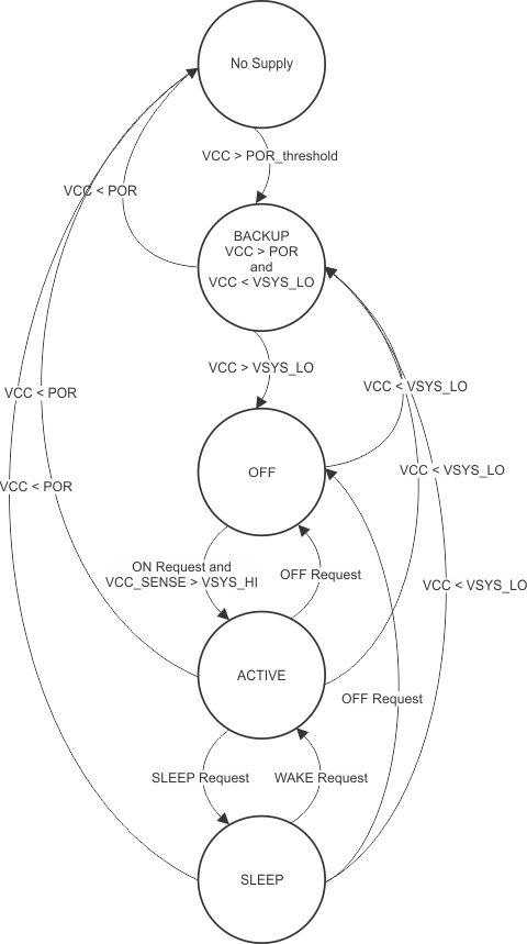
 The power state-machine is defined through the following states:
- NO SUPPLY: The device is not powered by any energy source on the system power rail (VCC1 < POR).
- BACKUP: The device is not powered by a valid supply on the system power rail (VCC1 < VSYS_LO) (VCC > POR).
- OFF: The device is powered by a valid supply on the system power rail (VCC1 > VSYS_LO) and it is waiting for a start-up event or condition. All device resources are in the OFF state. The approximate time for device to arrive the OFF state from the NO SUPPLY state, without considering the rise time of VSYS and the settling time of the VSYS_LO comparator, is approximately 5.5 ms.
- ACTIVE: The device is powered by a valid supply on the system power rail (VCC1 > VSYS_LO) and has received a start-up event. It has switched to the ACTIVE state, having full capacity to supply the processor and other platform modules.
- SLEEP: The device is powered by a valid supply on the system power rail (VCC1 > VSYS_LO) and is in low-power mode. All configured resources are set to their low-power mode, which can be ON, SLEEP, or OFF depending on the specific resource setting. If a given resource is maintained active (ON) during low-power mode, then all its linked subsystems are automatically maintained active.
Figure 6-18 shows the state diagram for the power control state-machine.
 Figure 6-18 State Diagram for the Power Control State-Machine
 Power sequences define how a resource state switches between the OFF, ACTIVE, and SLEEP states, but they have no effect during the NO SUPPLY or BACKUP states. The EPC supervises the system according to these power sequences, once the device is brought into the OFF state from a NO SUPPLY or BACKUP state. This is achieved automatically by internal hardware controlling the device before handing it over to the EPC.
The allowed power transitions are:
- OFF to ACTIVE (OFF2ACT)
- ACTIVE to OFF (ACT2OFF)
- ACTIVE to SLEEP (ACT2SLP)
- SLEEP to ACTIVE (SLP2ACT)
- SLEEP to OFF (SLP2OFF)
Each power transition consists of a sequence of one or several register accesses that controls the resources according to the EPC supervision. Because these sequences are stored in nonvolatile memory (OTP), they cannot be altered.