JAJSEF6L August 2013 – February 2019 TPS659038-Q1 , TPS659039-Q1
PRODUCTION DATA.
- 1 デバイスの概要
- 2 改訂履歴
- 3 Device Comparison
- 4 Pin Configuration and Functions
-
5 Specifications
- 5.1 Absolute Maximum Ratings
- 5.2 ESD Ratings
- 5.3 Recommended Operating Conditions
- 5.4 Thermal Information
- 5.5 Electrical Characteristics: Latch Up Rating
- 5.6 Electrical Characteristics: LDO Regulator
- 5.7 Electrical Characteristics: Dual-Phase (SMPS12 and SMPS45) and Triple-Phase (SMPS123 and SMPS457) Regulators
- 5.8 Electrical Characteristics: Stand-Alone Regulators (SMPS3, SMPS6, SMPS7, SMPS8, and SMPS9)
- 5.9 Electrical Characteristics: Reference Generator (Bandgap)
- 5.10 Electrical Characteristics: 16-MHz Crystal Oscillator, 32-kHz RC Oscillator, and Output Buffers
- 5.11 Electrical Characteristics: DC-DC Clock Sync
- 5.12 Electrical Characteristics: 12-Bit Sigma-Delta ADC
- 5.13 Electrical Characteristics: Thermal Monitoring and Shutdown
- 5.14 Electrical Characteristics: System Control Thresholds
- 5.15 Electrical Characteristics: Current Consumption
- 5.16 Electrical Characteristics: Digital Input Signal Parameters
- 5.17 Electrical Characteristics: Digital Output Signal Parameters
- 5.18 Electrical Characteristics: I/O Pullup and Pulldown Resistance
- 5.19 I2C Interface Timing Requirements
- 5.20 SPI Timing Requirements
- 5.21 Typical Characteristics
-
6 Detailed Description
- 6.1 Overview
- 6.2 Functional Block Diagrams
- 6.3
Feature Description
- 6.3.1 Power Management
- 6.3.2
Power Resources (Step-Down and Step-Up SMPS Regulators, LDOs)
- 6.3.2.1
Step-Down Regulators
- 6.3.2.1.1 Sync Clock Functionality
- 6.3.2.1.2 Output Voltage and Mode Selection
- 6.3.2.1.3 Current Monitoring and Short Circuit Detection
- 6.3.2.1.4 POWERGOOD
- 6.3.2.1.5 DVS-Capable Regulators
- 6.3.2.1.6 Non DVS-Capable Regulators
- 6.3.2.1.7 Step-Down Converters SMPS12 and SMPS123
- 6.3.2.1.8 Step-Down Converter SMPS45 and SMPS457
- 6.3.2.1.9 Step-Down Converters SMPS3, SMPS6, SMPS7, SMPS8, and SMPS9
- 6.3.2.2 LDOs – Low Dropout Regulators
- 6.3.2.1
Step-Down Regulators
- 6.3.3 Long-Press Key Detection
- 6.3.4 RTC
- 6.3.5 GPADC – 12-Bit Sigma-Delta ADC
- 6.3.6 General-Purpose I/Os (GPIO Terminals)
- 6.3.7 Thermal Monitoring
- 6.3.8 Interrupts
- 6.3.9 Control Interfaces
- 6.3.10 Device Identification
- 6.4 Device Functional Modes
-
7 Application and Implementation
- 7.1 Application Information
- 7.2
Typical Application
- 7.2.1 Design Requirements
- 7.2.2 Detailed Design Procedure
- 7.2.3 Application Curves
- 8 Power Supply Recommendations
- 9 Layout
- 10デバイスおよびドキュメントのサポート
- 11メカニカル、パッケージ、および注文情報
パッケージ・オプション
デバイスごとのパッケージ図は、PDF版データシートをご参照ください。
メカニカル・データ(パッケージ|ピン)
- ZWS|169
サーマルパッド・メカニカル・データ
発注情報
6.3.2.1.1 Sync Clock Functionality
The TPS65903x-Q1 device contains a SYNCDCDC input to sync DC-DCs with the external clock.
In forced PWM mode, SMPSs are synchronized on an external input clock (SYNCDCDC) whereas in ECO-mode, or if the SYNCDCDC pin is grounded, the switching frequency is based on an internal RC oscillator. The clock generated from the internal RC oscillator can be output through GPIO5 to provide synchronization clock to external SMPSs. For PWM mode, a PLL is present to buffer the external input clock to create nine clock signals for the nine SMPSs with different phases.
The sync clock dither specification parameters are based on a triangular dither pattern, but other patterns that comply with the minimum and maximum sync frequency range and the maximum dither slope can also be used.
 Figure 6-2 Sync Clock Range and Dither
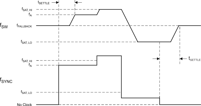
 The ollowing figure shows ƒSYNC, the frequency of SYNCDCDC input clock and ƒS, the frequency of PLL output signal.
When there is no clock present on SYNCDCDC ball, the PLL generates a clock with a frequency equal to ƒFALLBACK.
If a clock is present on SYNCDCDC ball with a frequency between ƒSAT,LO and ƒSAT,HI, then the PLL is synchronised on SYNCDCDC clock and generates a clock with frequency equal to fSYNC.
If ƒSYNC is higher than ƒSAT,HI, then the PLL generates a clock with a frequency equal to ƒSAT,HI.
If fSYNC is smaller than ƒSAT,LO, then the PLL generates a clock with a frequency equal to ƒSAT,LO.
 Figure 6-3 Sync Clock Saturation and Frequency Fallback