JAJSDU8C March 2016 – February 2019 TPS65916
PRODUCTION DATA.
- 1デバイスの概要
- 2改訂履歴
- 3Pin Configuration and Functions
-
4Specifications
- 4.1 Absolute Maximum Ratings
- 4.2 ESD Ratings
- 4.3 Recommended Operating Conditions
- 4.4 Thermal Information
- 4.5 Electrical Characteristics — LDO Regulators
- 4.6 Electrical Characteristics — SMPS1&2 in Dual-Phase Configuration
- 4.7 Electrical Characteristics — SMPS1, SMPS2, SMPS3, SMPS4, and SMPS5 Stand-Alone Regulators
- 4.8 Electrical Characteristics — Reference Generator (Bandgap)
- 4.9 Electrical Characteristics — 32-kHz RC Oscillators and SYNCCLKOUT Output Buffers
- 4.10 Electrical Characteristics — 12-Bit Sigma-Delta ADC
- 4.11 Electrical Characteristics — Thermal Monitoring and Shutdown
- 4.12 Electrical Characteristics — System Control Thresholds
- 4.13 Electrical Characteristics — Current Consumption
- 4.14 Electrical Characteristics — Digital Input Signal Parameters
- 4.15 Electrical Characteristics — Digital Output Signal Parameters
- 4.16 I/O Pullup and Pulldown Characteristics
- 4.17 Electrical Characteristics — I2C Interface
- 4.18 Timing Requirements — I2C Interface
- 4.19 Timing Requirements — SPI
- 4.20 Switching Characteristics — LDO Regulators
- 4.21 Switching Characteristics — SMPS1&2 in Dual-Phase Configuration
- 4.22 Switching Characteristics — SMPS1, SMPS2, SMPS3, SMPS4, and SMPS5 Stand-Alone Regulators
- 4.23 Switching Characteristics — Reference Generator (Bandgap)
- 4.24 Switching Characteristics — PLL for SMPS Clock Generation
- 4.25 Switching Characteristics — 32-kHz RC Oscillators and SYNCCLKOUT Output Buffers
- 4.26 Switching Characteristics — 12-Bit Sigma-Delta ADC
- 4.27 Typical Characteristics
-
5Detailed Description
- 5.1 Overview
- 5.2 Functional Block Diagram
- 5.3 Device State Machine
- 5.4
Power Resources (Step-Down and Step-Up SMPS Regulators, LDOs)
- 5.4.1 Step-Down Regulators
- 5.4.2 Low Dropout Regulators (LDOs)
- 5.5 SMPS and LDO Input Supply Connections
- 5.6 First Supply Detection
- 5.7 Long-Press Key Detection
- 5.8 12-Bit Sigma-Delta General-Purpose ADC (GPADC)
- 5.9 General-Purpose I/Os (GPIO Pins)
- 5.10 Thermal Monitoring
- 5.11 Interrupts
- 5.12 Control Interfaces
- 5.13 OTP Configuration Memory
- 5.14 Watchdog Timer (WDT)
- 5.15 System Voltage Monitoring
- 5.16 Register Map
- 5.17 Device Identification
- 6Applications, Implementation, and Layout
- 7デバイスおよびドキュメントのサポート
- 8メカニカル、パッケージ、および注文情報
5.4.1.4 POWERGOOD
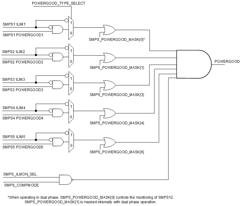
The TPS65916 device includes an external POWERGOOD pin which indicates if the outputs of the SMPS are within the acceptable range of the programmed output voltage, and if the current loading for the SMPS is within the range of the current limit. Users can select whether POWERGOOD reports the result of both voltage and current monitoring or only current monitoring. This selection applies to all SMPSs in the SMPS_POWERGOOD_MASK2 register.POWERGOOD_TYPE_SELECT register. When both the voltage and current are monitored, the POWERGOOD signal indicates whether or not all SMPS outputs are within a certain percentage, as specified by the VSMPSPG parameter, of the programmed value while the load current is below ILIM.
All POWERGOOD sources can be masked in the SMPS_POWERGOOD_MASK1 and SMPS_POWERGOOD_MASK2 registers. By default, only the SMPS1 rail (or SMPS12 rail if in dual phase) is monitored. When an SMPS is disabled, it should be masked in the SMPS_POWERGOOD_MASKx registers to prevent the SMPS from forcing the POWERGOOD pin to go inactive. When the SMPS voltage is transitioning from one target voltage to another because of a DVS command, voltage monitoring is internally masked and POWERGOOD is not impacted.
The GPADC result for SMPS output current monitoring can be included in POWERGOOD by setting the SMPS_COMPMODE bit to 1. The GPADC can monitor only one SMPS.
Figure 5-12 is the block diagram of the circuitry which constructs the logic output of the POWERGOOD pin.
CAUTION
When operating in dual phase, the SMPS12 current monitor may cause POWERGOOD to change to a low level (with default polarity) when transitioning from dual phase operation to single phase operation. TI recommends masking SMPS12 as a POWERGOOD source, using SMPS_POWERGOOD_MASK1, or debouncing the POWERGOOD signal if this POWERGOOD toggle is not desired in the application design.
 Figure 5-12 POWERGOOD Block Diagram