JAJSGV4D July 2015 – February 2019 TPS65917-Q1
PRODUCTION DATA.
- 1デバイスの概要
- 2改訂履歴
- 3Pin Configuration and Functions
-
4Specifications
- 4.1 Absolute Maximum Ratings
- 4.2 ESD Ratings
- 4.3 Recommended Operating Conditions
- 4.4 Thermal Information
- 4.5 Electrical Characteristics — LDO Regulators
- 4.6 Electrical Characteristics — SMPS1&2 in Dual-Phase Configuration
- 4.7 Electrical Characteristics — SMPS1, SMPS2, SMPS3, SMPS4, and SMPS5 Stand-Alone Regulators
- 4.8 Electrical Characteristics — Reference Generator (Bandgap)
- 4.9 Electrical Characteristics — 32-kHz RC Oscillators and SYNCCLKOUT Output Buffers
- 4.10 Electrical Characteristics — 12-Bit Sigma-Delta ADC
- 4.11 Electrical Characteristics — Thermal Monitoring and Shutdown
- 4.12 Electrical Characteristics — System Control Thresholds
- 4.13 Electrical Characteristics — Current Consumption
- 4.14 Electrical Characteristics — Digital Input Signal Parameters
- 4.15 Electrical Characteristics — Digital Output Signal Parameters
- 4.16 I/O Pullup and Pulldown Characteristics
- 4.17 Electrical Characteristics — I2C Interface
- 4.18 Timing Requirements — I2C Interface
- 4.19 Timing Requirements — SPI
- 4.20 Switching Characteristics — LDO Regulators
- 4.21 Switching Characteristics — SMPS1&2 in Dual-Phase Configuration
- 4.22 Switching Characteristics — SMPS1, SMPS2, SMPS3, SMPS4, and SMPS5 Stand-Alone Regulators
- 4.23 Switching Characteristics — Reference Generator (Bandgap)
- 4.24 Switching Characteristics — PLL for SMPS Clock Generation
- 4.25 Switching Characteristics — 32-kHz RC Oscillators and SYNCCLKOUT Output Buffers
- 4.26 Switching Characteristics — 12-Bit Sigma-Delta ADC
- 4.27 Typical Characteristics
-
5Detailed Description
- 5.1 Overview
- 5.2 Functional Block Diagram
- 5.3 Device State Machine
- 5.4
Power Resources (Step-Down and Step-Up SMPS Regulators, LDOs)
- 5.4.1 Step-Down Regulators
- 5.4.2 Low Dropout Regulators (LDOs)
- 5.5 SMPS and LDO Input Supply Connections
- 5.6 First Supply Detection
- 5.7 Long-Press Key Detection
- 5.8 12-Bit Sigma-Delta General-Purpose ADC (GPADC)
- 5.9 General-Purpose I/Os (GPIO Pins)
- 5.10 Thermal Monitoring
- 5.11 Interrupts
- 5.12 Control Interfaces
- 5.13 OTP Configuration Memory
- 5.14 Watchdog Timer (WDT)
- 5.15 System Voltage Monitoring
- 5.16 Register Map
- 5.17 Device Identification
- 6Applications, Implementation, and Layout
- 7デバイスおよびドキュメントのサポート
- 8メカニカル、パッケージ、および注文情報
パッケージ・オプション
デバイスごとのパッケージ図は、PDF版データシートをご参照ください。
メカニカル・データ(パッケージ|ピン)
- RGZ|48
サーマルパッド・メカニカル・データ
発注情報
6.2.2.6.1 Meeting the Power-Down Sequence
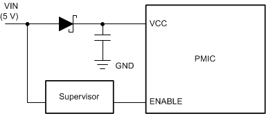
To prevent a sequencing violation, it is important to block reverse current and implement a disable signal to the PMIC. A Schottky diode can block reverse current when the input is removed. Additionally, capacitors can help maintain the input voltage level while the power-down sequence occurs. Depending on the system design, there are a couple ways to implement a disable signal.
For a system where the TPS65917-Q1 is powered by the system input voltage, a supervisor can be used to create a logic signal, indicating if the power is at a good level. An example of this solution is shown in Figure 6-2.
 Figure 6-2 Supporting Uncontrolled Power Down When the PMIC is Supplied by the System Input Voltage
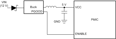
 An alternative solution is possible when a pre-regulator is present. In the case of the pre-regulator, the pre-regulator output capacitance can also act as the energy storage to maintain VCCA for the necessary time. The total supply capacitance should be calculated to support the worst-case leakage current during power down so that the voltage is maintained until the power-down sequence completes. Figure 6-3 shows an example of this configuration.
 Figure 6-3 Supporting Uncontrolled Power Down when the PMIC is Supplied by a Preregulator
 To determine the capacitance needed at the output of the pre-regulator, use Equation 1. This equation is used to ensure that the power down sequence is complete before the device is disabled.
where
- C is total capacitance on VCCA, including preregulator output capacitance and PMIC input capacitance
- I is the total current on the PMIC input supply
- ΔT is the time it takes the power-down sequence to complete
- VCCA is the voltage at the VCCA pin
- VSYS_LO is the threshold where the device is disabled