JAJSGV4D July 2015 – February 2019 TPS65917-Q1
PRODUCTION DATA.
- 1デバイスの概要
- 2改訂履歴
- 3Pin Configuration and Functions
-
4Specifications
- 4.1 Absolute Maximum Ratings
- 4.2 ESD Ratings
- 4.3 Recommended Operating Conditions
- 4.4 Thermal Information
- 4.5 Electrical Characteristics — LDO Regulators
- 4.6 Electrical Characteristics — SMPS1&2 in Dual-Phase Configuration
- 4.7 Electrical Characteristics — SMPS1, SMPS2, SMPS3, SMPS4, and SMPS5 Stand-Alone Regulators
- 4.8 Electrical Characteristics — Reference Generator (Bandgap)
- 4.9 Electrical Characteristics — 32-kHz RC Oscillators and SYNCCLKOUT Output Buffers
- 4.10 Electrical Characteristics — 12-Bit Sigma-Delta ADC
- 4.11 Electrical Characteristics — Thermal Monitoring and Shutdown
- 4.12 Electrical Characteristics — System Control Thresholds
- 4.13 Electrical Characteristics — Current Consumption
- 4.14 Electrical Characteristics — Digital Input Signal Parameters
- 4.15 Electrical Characteristics — Digital Output Signal Parameters
- 4.16 I/O Pullup and Pulldown Characteristics
- 4.17 Electrical Characteristics — I2C Interface
- 4.18 Timing Requirements — I2C Interface
- 4.19 Timing Requirements — SPI
- 4.20 Switching Characteristics — LDO Regulators
- 4.21 Switching Characteristics — SMPS1&2 in Dual-Phase Configuration
- 4.22 Switching Characteristics — SMPS1, SMPS2, SMPS3, SMPS4, and SMPS5 Stand-Alone Regulators
- 4.23 Switching Characteristics — Reference Generator (Bandgap)
- 4.24 Switching Characteristics — PLL for SMPS Clock Generation
- 4.25 Switching Characteristics — 32-kHz RC Oscillators and SYNCCLKOUT Output Buffers
- 4.26 Switching Characteristics — 12-Bit Sigma-Delta ADC
- 4.27 Typical Characteristics
-
5Detailed Description
- 5.1 Overview
- 5.2 Functional Block Diagram
- 5.3 Device State Machine
- 5.4
Power Resources (Step-Down and Step-Up SMPS Regulators, LDOs)
- 5.4.1 Step-Down Regulators
- 5.4.2 Low Dropout Regulators (LDOs)
- 5.5 SMPS and LDO Input Supply Connections
- 5.6 First Supply Detection
- 5.7 Long-Press Key Detection
- 5.8 12-Bit Sigma-Delta General-Purpose ADC (GPADC)
- 5.9 General-Purpose I/Os (GPIO Pins)
- 5.10 Thermal Monitoring
- 5.11 Interrupts
- 5.12 Control Interfaces
- 5.13 OTP Configuration Memory
- 5.14 Watchdog Timer (WDT)
- 5.15 System Voltage Monitoring
- 5.16 Register Map
- 5.17 Device Identification
- 6Applications, Implementation, and Layout
- 7デバイスおよびドキュメントのサポート
- 8メカニカル、パッケージ、および注文情報
パッケージ・オプション
デバイスごとのパッケージ図は、PDF版データシートをご参照ください。
メカニカル・データ(パッケージ|ピン)
- RGZ|48
サーマルパッド・メカニカル・データ
発注情報
6.3.1 Layout Guidelines
As in every switch-mode-supply design, general layout rules apply:
- Use a solid ground-plane for the power ground (PGND)
- Connect those grounds at a star-point that is located ideally underneath the device.
- Place input capacitors as close as possible to the input pins of the device. This placement is paramount and more important than the output-loop.
- Place the inductor and output capacitor as close as possible to the phase node (or switch-node) of the device.
- Keep the loop-area formed by the phase-node, inductor, output-capacitor, and PGND as small as possible.
- For traces and vias on power-lines, keep inductance and resistance as small as possible by using wide traces. Avoid switching layers but, if needed, use plenty of vias.
The goal of these guidelines is a layout that minimizes emissions, maximizes EMI immunity, and maintains a safe operating area (SOA) for the device.
To minimize the spiking at the phase-node for both the high-side (VIN to SWx) and low-side (SWx to PGND), the decoupling of VIN is the most important guideline. Appropriate decoupling and thorough layout should ensure that the spikes never exceed 7V across the high-side and low-side FETs.
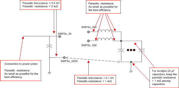
Figure 6-9 shows a set of guidelines regarding parasitic inductance and resistance that are recommended.
 Figure 6-9 Parasitic Inductance and Resistance
 Table 6-3 lists the maximum allowable parasitic (inductance measured at 100 MHz) and the achievable values in an optimized layout.
Table 6-3 Maximum Allowable Parasitic
| CONNECTION | MAXIMUM ALLOWABLE INDUCTANCE | MAXIMUM ALLOWABLE RESISTANCE | OPTIMIZED LAYOUT (EVM) INDUCTANCE | OPTIMIZED LAYOUT (EVM) RESISTANCE | ||
|---|---|---|---|---|---|---|
| PowerPlane to CIN | N/A | N/A for SOA
Maintain a low resistance value for efficiency |
N/A | N/A for SOA
Maintain a low resistance value for efficiency |
||
| CIN to SMPSx_IN | 0.5 nH | 2 mΩ | SMPS1 | 0.2 nH | SMPS1 | 1.1 mΩ |
| SMPS2 | 0.2 nH | SMPS2 | 1.6 mΩ | |||
| SMPS3 | 0.2 nH | SMPS3 | 1.5 mΩ | |||
| SMPS4 | 0.2 nH | SMPS4 | 1.8 mΩ | |||
| SMPS5 | 0.2 nH | SMPS5 | 1.5 mΩ | |||
| CIN to PGND | 0.5 nH | 2 mΩ | SMPS1 | 0.3 nH | SMPS1 | 0.4 mΩ |
| SMPS2 | 0.3 nH | SMPS2 | 0.4 mΩ | |||
| SMPS3 | 0.4 nH | SMPS3 | 0.5 mΩ | |||
| SMPS4 | 0.3 nH | SMPS4 | 0.6 mΩ | |||
| SMPS5 | 0.4 nH | SMPS5 | 0.5 mΩ | |||
| SMPSx_SW to inductor | N/A | N/A for SOA
Maintain a low resistance value for efficiency |
N/A | SMPS1 | 1 mΩ | |
| SMPS2 | 0.7 mΩ | |||||
| SMPS3 | 1 mΩ | |||||
| SMPS4 | 0.7 mΩ | |||||
| SMPS5 | 1.4 mΩ | |||||
| Inductor to COUT | N/A | N/A for SOA
Maintain a low resistance value for efficiency |
N/A | N/A for SOA
Maintain a low resistance value for efficiency |
||
| COUT to GND | Use dedicated GND plane to keep inductance low | 1 mΩ | SMPS1 | 0.8 nH | SMPS1 | 0.7 mΩ |
| SMPS2 | 0.6 nH | SMPS2 | 0.8 mΩ | |||
| SMPS3 | 0.5 nH | SMPS3 | 0.6 mΩ | |||
| SMPS4 | 0.4 nH | SMPS4 | 0.6 mΩ | |||
| SMPS5 | 0.5 nH | SMPS5 | 0.5 mΩ | |||
| GND (CIN) to GND (COUT) | Use dedicated GND plane to keep inductance low | 1 mΩ | Use dedicated GND plane to keep inductance low | mΩ | ||
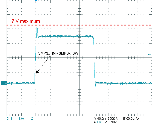
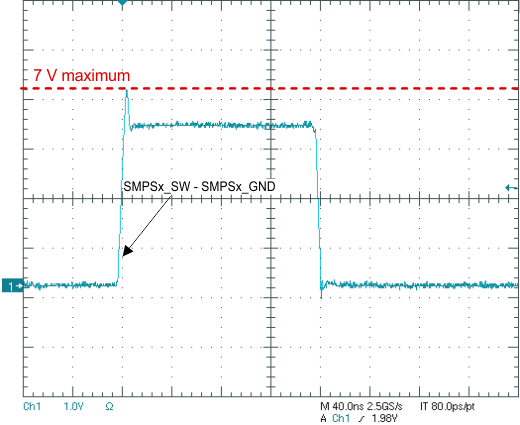
Texas Instruments recommends measuring the voltages across the high-side FET (voltage at SMPSx_IN versus SMPSx_SW) and the low-side FET (SMPSx_SW versus PGND) with a high bandwidth, high sampling-rate scope with a low-capacitance probe (ideally a differential probe). Measure the voltages as close as possible to the device pins and verify the amplitude of the spikes. A small-loop ground connection to PGND is essential.
When measuring the voltage difference between the SMPSx_IN and SMPSx_SW pins, there should be a maximum of 7 V when measuring at the pins. Similarly, when measuring the voltage difference between the SMPSx_SW and PGND pins, there should be a maximum of 7 V when measuring at the pins.
For more information on cursor-positioning, see Figure 6-10 and Figure 6-11.

