JAJSGV4D July 2015 – February 2019 TPS65917-Q1
PRODUCTION DATA.
- 1デバイスの概要
- 2改訂履歴
- 3Pin Configuration and Functions
-
4Specifications
- 4.1 Absolute Maximum Ratings
- 4.2 ESD Ratings
- 4.3 Recommended Operating Conditions
- 4.4 Thermal Information
- 4.5 Electrical Characteristics — LDO Regulators
- 4.6 Electrical Characteristics — SMPS1&2 in Dual-Phase Configuration
- 4.7 Electrical Characteristics — SMPS1, SMPS2, SMPS3, SMPS4, and SMPS5 Stand-Alone Regulators
- 4.8 Electrical Characteristics — Reference Generator (Bandgap)
- 4.9 Electrical Characteristics — 32-kHz RC Oscillators and SYNCCLKOUT Output Buffers
- 4.10 Electrical Characteristics — 12-Bit Sigma-Delta ADC
- 4.11 Electrical Characteristics — Thermal Monitoring and Shutdown
- 4.12 Electrical Characteristics — System Control Thresholds
- 4.13 Electrical Characteristics — Current Consumption
- 4.14 Electrical Characteristics — Digital Input Signal Parameters
- 4.15 Electrical Characteristics — Digital Output Signal Parameters
- 4.16 I/O Pullup and Pulldown Characteristics
- 4.17 Electrical Characteristics — I2C Interface
- 4.18 Timing Requirements — I2C Interface
- 4.19 Timing Requirements — SPI
- 4.20 Switching Characteristics — LDO Regulators
- 4.21 Switching Characteristics — SMPS1&2 in Dual-Phase Configuration
- 4.22 Switching Characteristics — SMPS1, SMPS2, SMPS3, SMPS4, and SMPS5 Stand-Alone Regulators
- 4.23 Switching Characteristics — Reference Generator (Bandgap)
- 4.24 Switching Characteristics — PLL for SMPS Clock Generation
- 4.25 Switching Characteristics — 32-kHz RC Oscillators and SYNCCLKOUT Output Buffers
- 4.26 Switching Characteristics — 12-Bit Sigma-Delta ADC
- 4.27 Typical Characteristics
-
5Detailed Description
- 5.1 Overview
- 5.2 Functional Block Diagram
- 5.3 Device State Machine
- 5.4
Power Resources (Step-Down and Step-Up SMPS Regulators, LDOs)
- 5.4.1 Step-Down Regulators
- 5.4.2 Low Dropout Regulators (LDOs)
- 5.5 SMPS and LDO Input Supply Connections
- 5.6 First Supply Detection
- 5.7 Long-Press Key Detection
- 5.8 12-Bit Sigma-Delta General-Purpose ADC (GPADC)
- 5.9 General-Purpose I/Os (GPIO Pins)
- 5.10 Thermal Monitoring
- 5.11 Interrupts
- 5.12 Control Interfaces
- 5.13 OTP Configuration Memory
- 5.14 Watchdog Timer (WDT)
- 5.15 System Voltage Monitoring
- 5.16 Register Map
- 5.17 Device Identification
- 6Applications, Implementation, and Layout
- 7デバイスおよびドキュメントのサポート
- 8メカニカル、パッケージ、および注文情報
パッケージ・オプション
デバイスごとのパッケージ図は、PDF版データシートをご参照ください。
メカニカル・データ(パッケージ|ピン)
- RGZ|48
サーマルパッド・メカニカル・データ
発注情報
5.3.1 Embedded Power Controller
The EPC is composed of the following three main modules:
- An event arbitration module that is used to prioritize ON, OFF, WAKE, and SLEEP requests.
- A power state-machine that is used to determine which power sequence to execute based on the system state (supplies, temperature, and so forth) and requested transition (from the event arbitration module).
- A power sequencer that fetches the selected power sequence from OTP and executes the sequence. The power sequencer sets up and controls all resources accordingly, based on the definition of each sequence.
Figure 5-1 shows the EPC block diagram.
 Figure 5-1 EPC Block Diagram
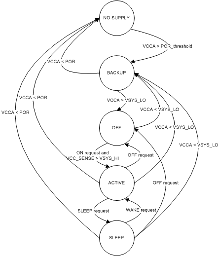
 The power state-machine is defined through the following states:
- NO SUPPLYThe device is not powered by a valid energy source on the system power rail (VCCA < POR).
- BACKUPThe device is powered by a valid supply on the system power rail which is above power-on reset (POR) threshold but below the system low threshold (POR < VCCA < VSYS_LO).
- OFFThe device is powered by a valid supply on the system power rail (VCCA > VSYS_LO) and is waiting for a start-up event or condition. All device resources, except VRTC, are in the OFF state.
- ACTIVEThe device is powered by a valid supply on the system power rail (VCC_SENSE > VSYS_HI) and has received a start-up event. The device has switched to the ACTIVE state and has full capacity to supply the processor and other platform modules.
- SLEEPThe device is powered by a valid supply on the system power rail (VCCA > VSYS_LO) and is in low-power mode. All configured resources are set to the low-power mode, which can be ON, SLEEP, or OFF depending on the specific resource setting. If a given resource is maintained active (ON) during low-power mode, then all linked subsystems are automatically maintained active.
Figure 5-2 shows the state diagram for the power control state-machine.
 Figure 5-2 State Diagram for the Power Control State-Machine
 Power sequences define how a resource state switches between the OFF, ACTIVE, and SLEEP states, but these sequences have no effect during the NO SUPPLY or BACKUP states. When the device is brought into the OFF state from a NO SUPPLY or BACKUP state, internal hardware manages the state transition automatically before the EPC takes control of the device power sequencing as the device arrives the OFF state.
The allowed power transitions include the following:
- OFF to ACTIVE (OFF2ACT)
- ACTIVE to OFF (ACT2OFF)
- ACTIVE to SLEEP (ACT2SLP)
- SLEEP to ACTIVE (SLP2ACT)
- SLEEP to OFF (SLP2OFF)
Each power transition consists of a sequence of one or several register accesses that controls the resources according to the EPC supervision. Because these sequences are stored in nonvolatile memory (OTP), these sequences cannot be altered.
As an additional safety feature, an error detection routine of the OTP bit integrity is available with this device. If enabled, this routine is executed to compare the current OTP values with the preprogrammed values at the beginning of every OFF2ACT power sequence. When an OTP bit integrity error is detected, the OTP register, CRC_CONTROL, can be preprogramed to select the following options:
- Skip Error Detection and execute all power sequence
- Execute Error Detection and execute all power-up sequence, even if an error is detected
- Execute Error Detection. If an error is detected, execute power-up sequence until the VIO supply rail is up
- Execute Error Detection. If an error is detected, stop power-up sequence altogether
When an error is detected, an interrupt (INT2.OTP_ERROR) is sent to the host processor regardless of the CRC_CONTROL setting.