JAJSGV4D July 2015 – February 2019 TPS65917-Q1
PRODUCTION DATA.
- 1デバイスの概要
- 2改訂履歴
- 3Pin Configuration and Functions
-
4Specifications
- 4.1 Absolute Maximum Ratings
- 4.2 ESD Ratings
- 4.3 Recommended Operating Conditions
- 4.4 Thermal Information
- 4.5 Electrical Characteristics — LDO Regulators
- 4.6 Electrical Characteristics — SMPS1&2 in Dual-Phase Configuration
- 4.7 Electrical Characteristics — SMPS1, SMPS2, SMPS3, SMPS4, and SMPS5 Stand-Alone Regulators
- 4.8 Electrical Characteristics — Reference Generator (Bandgap)
- 4.9 Electrical Characteristics — 32-kHz RC Oscillators and SYNCCLKOUT Output Buffers
- 4.10 Electrical Characteristics — 12-Bit Sigma-Delta ADC
- 4.11 Electrical Characteristics — Thermal Monitoring and Shutdown
- 4.12 Electrical Characteristics — System Control Thresholds
- 4.13 Electrical Characteristics — Current Consumption
- 4.14 Electrical Characteristics — Digital Input Signal Parameters
- 4.15 Electrical Characteristics — Digital Output Signal Parameters
- 4.16 I/O Pullup and Pulldown Characteristics
- 4.17 Electrical Characteristics — I2C Interface
- 4.18 Timing Requirements — I2C Interface
- 4.19 Timing Requirements — SPI
- 4.20 Switching Characteristics — LDO Regulators
- 4.21 Switching Characteristics — SMPS1&2 in Dual-Phase Configuration
- 4.22 Switching Characteristics — SMPS1, SMPS2, SMPS3, SMPS4, and SMPS5 Stand-Alone Regulators
- 4.23 Switching Characteristics — Reference Generator (Bandgap)
- 4.24 Switching Characteristics — PLL for SMPS Clock Generation
- 4.25 Switching Characteristics — 32-kHz RC Oscillators and SYNCCLKOUT Output Buffers
- 4.26 Switching Characteristics — 12-Bit Sigma-Delta ADC
- 4.27 Typical Characteristics
-
5Detailed Description
- 5.1 Overview
- 5.2 Functional Block Diagram
- 5.3 Device State Machine
- 5.4
Power Resources (Step-Down and Step-Up SMPS Regulators, LDOs)
- 5.4.1 Step-Down Regulators
- 5.4.2 Low Dropout Regulators (LDOs)
- 5.5 SMPS and LDO Input Supply Connections
- 5.6 First Supply Detection
- 5.7 Long-Press Key Detection
- 5.8 12-Bit Sigma-Delta General-Purpose ADC (GPADC)
- 5.9 General-Purpose I/Os (GPIO Pins)
- 5.10 Thermal Monitoring
- 5.11 Interrupts
- 5.12 Control Interfaces
- 5.13 OTP Configuration Memory
- 5.14 Watchdog Timer (WDT)
- 5.15 System Voltage Monitoring
- 5.16 Register Map
- 5.17 Device Identification
- 6Applications, Implementation, and Layout
- 7デバイスおよびドキュメントのサポート
- 8メカニカル、パッケージ、および注文情報
パッケージ・オプション
デバイスごとのパッケージ図は、PDF版データシートをご参照ください。
メカニカル・データ(パッケージ|ピン)
- RGZ|48
サーマルパッド・メカニカル・データ
発注情報
5.8 12-Bit Sigma-Delta General-Purpose ADC (GPADC)
The features of the GPADC include the following:
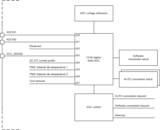
The GPADC consists of a 12-bit sigma-delta ADC combined with a 8-input analog multiplexer. The running frequency of the GPADC is 2.5MHz. The GPADC lets the host processor monitor analog signals using analog-to-digital conversion on the input source. After the conversion is complete, an interrupt is generated to signal the host processor that the result of the conversion is ready to be accessed through the I2C interface.
The GPADC supports 8 analog inputs. Two of these inputs are available on external pins and the remaining inputs are dedicated to VSYS supply voltage monitoring and internal resource monitoring.
Figure 5-15 shows the block diagram of the GPADC.
 Figure 5-15 Block Diagram of the GPADC
 The conversion requests are initiated by the host processor either by software through the I2C or by periodical measurements.
Two kinds of conversion requests occur with the following priority:
- Asynchronous conversion request (SW), see Section 5.8.1
- Periodic conversion (AUTO), see Section 5.8.2
Table 5-9 lists the GPADC channel assignments.
Use Equation 3 to convert from the GPADC code to the internal die temperature using GPADC channels 5 and 6.

Table 5-9 GPADC Channel Assignments
| CHANNEL | TYPE | INPUT VOLTAGE
FULL RANGE (1) |
INPUT VOLTAGE
PERFORMANCE RANGE(2) |
SCALER | OPERATION |
|---|---|---|---|---|---|
| 0 (ADCIN1) | External(3) | 0 to 1.25 V | 0.01 to 1.215 V | No | General purpose |
| 1 (ADCIN2) | External(3) | 0 to 1.25 V | 0.01 to 1.215 V | No | General purpose |
| 2 | Reserved | ||||
| 3 (VCC_SENSE) | Internal | 2.5 to 5 V when HIGH_VCC_SENSE = 0
2.3 V to (VCCA – 1 V) when HIGH_VCC_SENSE = 1 |
2.5 to 4.86 V when HIGH_VCC_SENSE = 0
2.3 V to (VCCA – 1 V) when HIGH_VCC_SENSE = 1 |
4 | System supply voltage (VCC_SENSE) |
| 4 | Internal | 0 to 1.25 V | No | DC-DC current probe | |
| 5 | Internal | 0 to 1.25 V | 0 to 1.215 V | No | PMIC internal die temperature 1 |
| 6 | Internal | 0 to 1.25 V | 0 to 1.215 V | No | PMIC internal die temperature 2 |
| 7 | Internal | 0 to VCCA V | 0.055 to VCCA V | 5 | Test network |