JAJSGV4D July   2015  – February 2019 TPS65917-Q1

PRODUCTION DATA.  

  1. 1デバイスの概要
    1. 1.1 特長
    2. 1.2 アプリケーション
    3. 1.3 概要
    4. 1.4 チャネル 1 の機能図
  2. 2改訂履歴
  3. 3Pin Configuration and Functions
    1. 3.1 Pin Attributes
      1.      Pin Attributes
    2. 3.2 Signal Descriptions
  4. 4Specifications
    1. 4.1  Absolute Maximum Ratings
    2. 4.2  ESD Ratings
    3. 4.3  Recommended Operating Conditions
    4. 4.4  Thermal Information
    5. 4.5  Electrical Characteristics — LDO Regulators
    6. 4.6  Electrical Characteristics — SMPS1&2 in Dual-Phase Configuration
    7. 4.7  Electrical Characteristics — SMPS1, SMPS2, SMPS3, SMPS4, and SMPS5 Stand-Alone Regulators
    8. 4.8  Electrical Characteristics — Reference Generator (Bandgap)
    9. 4.9  Electrical Characteristics — 32-kHz RC Oscillators and SYNCCLKOUT Output Buffers
    10. 4.10 Electrical Characteristics — 12-Bit Sigma-Delta ADC
    11. 4.11 Electrical Characteristics — Thermal Monitoring and Shutdown
    12. 4.12 Electrical Characteristics — System Control Thresholds
    13. 4.13 Electrical Characteristics — Current Consumption
    14. 4.14 Electrical Characteristics — Digital Input Signal Parameters
    15. 4.15 Electrical Characteristics — Digital Output Signal Parameters
    16. 4.16 I/O Pullup and Pulldown Characteristics
    17. 4.17 Electrical Characteristics — I2C Interface
    18. 4.18 Timing Requirements — I2C Interface
    19. 4.19 Timing Requirements — SPI
    20. 4.20 Switching Characteristics — LDO Regulators
    21. 4.21 Switching Characteristics — SMPS1&2 in Dual-Phase Configuration
    22. 4.22 Switching Characteristics — SMPS1, SMPS2, SMPS3, SMPS4, and SMPS5 Stand-Alone Regulators
    23. 4.23 Switching Characteristics — Reference Generator (Bandgap)
    24. 4.24 Switching Characteristics — PLL for SMPS Clock Generation
    25. 4.25 Switching Characteristics — 32-kHz RC Oscillators and SYNCCLKOUT Output Buffers
    26. 4.26 Switching Characteristics — 12-Bit Sigma-Delta ADC
    27. 4.27 Typical Characteristics
  5. 5Detailed Description
    1. 5.1  Overview
    2. 5.2  Functional Block Diagram
    3. 5.3  Device State Machine
      1. 5.3.1  Embedded Power Controller
      2. 5.3.2  State Transition Requests
        1. 5.3.2.1 ON Requests
        2. 5.3.2.2 OFF Requests
        3. 5.3.2.3 SLEEP and WAKE Requests
      3. 5.3.3  Power Sequences
      4. 5.3.4  Device Power Up Timing
      5. 5.3.5  Power-On Acknowledge
        1. 5.3.5.1 POWERHOLD Mode
        2. 5.3.5.2 AUTODEVON Mode
      6. 5.3.6  BOOT Configuration
        1. 5.3.6.1 Boot Pin Usage and Connection
      7. 5.3.7  Reset Levels
      8. 5.3.8  INT
      9. 5.3.9  Warm Reset
      10. 5.3.10 RESET_IN
    4. 5.4  Power Resources (Step-Down and Step-Up SMPS Regulators, LDOs)
      1. 5.4.1 Step-Down Regulators
        1. 5.4.1.1 Output Voltage and Mode Selection
        2. 5.4.1.2 Clock Generation for SMPS
        3. 5.4.1.3 Current Monitoring and Short Circuit Detection
        4. 5.4.1.4 POWERGOOD
        5. 5.4.1.5 DVS-Capable Regulators
          1. 5.4.1.5.1 Non DVS-Capable Regulators
        6. 5.4.1.6 Step-Down Converters SMPS1, SMPS2 or SMPS1&2
        7. 5.4.1.7 Step-Down Converters SMPS3, SMPS4, and SMPS5
      2. 5.4.2 Low Dropout Regulators (LDOs)
        1. 5.4.2.1 LDOVANA
        2. 5.4.2.2 LDOVRTC
        3. 5.4.2.3 LDO1 and LDO2
        4. 5.4.2.4 Low-Noise LDO (LDO5)
        5. 5.4.2.5 Other LDOs
    5. 5.5  SMPS and LDO Input Supply Connections
    6. 5.6  First Supply Detection
    7. 5.7  Long-Press Key Detection
    8. 5.8  12-Bit Sigma-Delta General-Purpose ADC (GPADC)
      1. 5.8.1 Asynchronous Conversion Request (SW)
      2. 5.8.2 Periodic Conversion (AUTO)
      3. 5.8.3 Calibration
    9. 5.9  General-Purpose I/Os (GPIO Pins)
    10. 5.10 Thermal Monitoring
      1. 5.10.1 Hot-Die Function (HD)
      2. 5.10.2 Thermal Shutdown
    11. 5.11 Interrupts
    12. 5.12 Control Interfaces
      1. 5.12.1 I2C Interfaces
        1. 5.12.1.1 I2C Implementation
        2. 5.12.1.2 F/S Mode Protocol
        3. 5.12.1.3 HS Mode Protocol
      2. 5.12.2 Serial Peripheral Interface (SPI)
        1. 5.12.2.1 SPI Modes
        2. 5.12.2.2 SPI Protocol
    13. 5.13 OTP Configuration Memory
    14. 5.14 Watchdog Timer (WDT)
    15. 5.15 System Voltage Monitoring
    16. 5.16 Register Map
      1. 5.16.1 Functional Register Mapping
    17. 5.17 Device Identification
  6. 6Applications, Implementation, and Layout
    1. 6.1 Application Information
    2. 6.2 Typical Application
      1. 6.2.1 Design Requirements
      2. 6.2.2 Detailed Design Procedure
        1. 6.2.2.1 SMPS Input Capacitors
        2. 6.2.2.2 SMPS Output Capacitors
        3. 6.2.2.3 SMPS Inductors
        4. 6.2.2.4 LDO Input Capacitors
        5. 6.2.2.5 LDO Output Capacitors
        6. 6.2.2.6 VCCA
          1. 6.2.2.6.1 Meeting the Power-Down Sequence
          2. 6.2.2.6.2 Maintaining Sufficient Input Voltage
        7. 6.2.2.7 VIO_IN
        8. 6.2.2.8 GPADC
      3. 6.2.3 Application Curves
    3. 6.3 Layout
      1. 6.3.1 Layout Guidelines
      2. 6.3.2 Layout Example
    4. 6.4 Power Supply Coupling and Bulk Capacitors
  7. 7デバイスおよびドキュメントのサポート
    1. 7.1 デバイス・サポート
      1. 7.1.1 Third-Party Products Disclaimer
      2. 7.1.2 デバイスの項目表記
    2. 7.2 ドキュメントのサポート
      1. 7.2.1 関連資料
    3. 7.3 ドキュメントの更新通知を受け取る方法
    4. 7.4 Community Resources
    5. 7.5 商標
    6. 7.6 静電気放電に関する注意事項
    7. 7.7 Glossary
  8. 8メカニカル、パッケージ、および注文情報

パッケージ・オプション

デバイスごとのパッケージ図は、PDF版データシートをご参照ください。

メカニカル・データ(パッケージ|ピン)
  • RGZ|48
サーマルパッド・メカニカル・データ
発注情報

Calibration

The GPADC channels are calibrated in the production line using a 2-point calibration method. The channels are measured with two known values (X1 and X2) and the difference (D1 and D2) to the ideal values (Y1 and Y2) are stored in the OTP memory. Figure 5-16 shows the principle of the calibration.
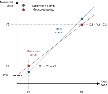
TPS65917-Q1 ADC_calibration_slvsco4.gifFigure 5-16 ADC Calibration Scheme

Some of the GPADC channels can use the same calibration data. Use Equation 4 and Equation 5 to calculate the corrected result.

Equation 4. Gain:TPS65917-Q1 eq_05_slia087.gif
Equation 5. Offset:TPS65917-Q1 eq_06_slia087.gif

If the measured code is a, the corrected code a' is calculated using Equation 6.

Equation 6. TPS65917-Q1 eq_07_slia087.gif

Table 5-10 lists the parameters, X1 and X2, and the register for D1 and D2 required in the calculation for all the channels.

Table 5-10 GPADC Calibration Parameters

CHANNEL X1 X2 D1 D2 COMMENTS
0, 1 2064 (0.63 V) 3112 (0.95 V) GPADC_TRIM1 GPADC_TRIM2
3 2064 (2.52 V) 3112 (3.8 V) GPADC_TRIM3 GPADC_TRIM4 When HIGH_VCC_SENSE = 0
3 2064 (2.52 V) 3112 (3.8 V) GPADC_TRIM5 GPADC_TRIM6 When HIGH_VCC_SENSE = 1