JAJSHC5B May   2019  – October 2022 TPS65987DDJ

PRODUCTION DATA  

  1. 特長
  2. アプリケーション
  3. 概要
  4. Revision History
  5. Pin Configuration and Functions
  6. Specifications
    1. 6.1  Absolute Maximum Ratings
    2. 6.2  ESD Ratings
    3. 6.3  Recommended Operating Conditions
    4. 6.4  Thermal Information
    5. 6.5  Power Supply Requirements and Characteristics
    6. 6.6  Power Consumption Characteristics
    7. 6.7  Power Switch Characteristics
    8. 6.8  Cable Detection Characteristics
    9. 6.9  USB-PD Baseband Signal Requirements and Characteristics
    10. 6.10 BC1.2 Characteristics
    11. 6.11 Thermal Shutdown Characteristics
    12. 6.12 Oscillator Characteristics
    13. 6.13 I/O Characteristics
    14. 6.14 I2C Requirements and Characteristics
    15. 6.15 SPI Controller Timing Requirements
    16. 6.16 HPD Timing Requirements
    17. 6.17 Typical Characteristics
  7. Parameter Measurement Information
  8. Detailed Description
    1. 8.1 Overview
    2. 8.2 Functional Block Diagram
    3. 8.3 Feature Description
      1. 8.3.1  USB-PD Physical Layer
        1. 8.3.1.1 USB-PD Encoding and Signaling
        2. 8.3.1.2 USB-PD Bi-Phase Marked Coding
        3. 8.3.1.3 USB-PD Transmit (TX) and Receive (Rx) Masks
        4. 8.3.1.4 USB-PD BMC Transmitter
        5. 8.3.1.5 USB-PD BMC Receiver
      2. 8.3.2  Power Management
        1. 8.3.2.1 Power-On And Supervisory Functions
        2. 8.3.2.2 VBUS LDO
        3. 8.3.2.3 Supply Switch Over
      3. 8.3.3  Port Power Switches
        1. 8.3.3.1 PP_HV Power Switch
          1. 8.3.3.1.1 PP_HV Overcurrent Clamp
          2. 8.3.3.1.2 PP_HV Overcurrent Protection
          3. 8.3.3.1.3 PP_HV OVP and UVP
          4. 8.3.3.1.4 PP_HV Reverse Current Protection
        2. 8.3.3.2 Schottky for Current Surge Protection
        3. 8.3.3.3 PP_EXT Power Path Control
        4. 8.3.3.4 PP_CABLE Power Switch
          1. 8.3.3.4.1 PP_CABLE Overcurrent Protection
          2. 8.3.3.4.2 PP_CABLE Input Good Monitor
        5. 8.3.3.5 VBUS Transition to VSAFE5V
        6. 8.3.3.6 VBUS Transition to VSAFE0V
      4. 8.3.4  Cable Plug and Orientation Detection
        1. 8.3.4.1 Configured as a DFP
        2. 8.3.4.2 Configured as a UFP
        3. 8.3.4.3 Configured as a DRP
        4. 8.3.4.4 Fast Role Swap Signaling
      5. 8.3.5  Dead Battery Operation
        1. 8.3.5.1 Dead Battery Advertisement
        2. 8.3.5.2 BUSPOWER (ADCIN1)
      6. 8.3.6  Battery Charger Detection and Advertisement
        1. 8.3.6.1 BC1.2 Data Contact Detect
        2. 8.3.6.2 BC1.2 Primary and Secondary Detection
        3. 8.3.6.3 Charging Downstream Port Advertisement
        4. 8.3.6.4 Dedicated Charging Port Advertisement
        5. 8.3.6.5 2.7-V Divider3 Mode Advertisement
        6. 8.3.6.6 1.2-V Mode Advertisement
        7. 8.3.6.7 DCP Auto Mode Advertisement
      7. 8.3.7  ADC
      8. 8.3.8  DisplayPort HPD
      9. 8.3.9  Digital Interfaces
        1. 8.3.9.1 General GPIO
        2. 8.3.9.2 I2C
        3. 8.3.9.3 SPI
      10. 8.3.10 Digital Core
      11. 8.3.11 I2C Interfaces
        1. 8.3.11.1 I2C Interface Description
        2. 8.3.11.2 I2C Clock Stretching
        3. 8.3.11.3 I2C Address Setting
        4. 8.3.11.4 Unique Address Interface
        5. 8.3.11.5 I2C Pin Address Setting (ADCIN2)
      12. 8.3.12 SPI Controller Interface
      13. 8.3.13 Thermal Shutdown
      14. 8.3.14 Oscillators
    4. 8.4 Device Functional Modes
      1. 8.4.1 Boot
      2. 8.4.2 Power States
  9. Application and Implementation
    1. 9.1 Application Information
    2. 9.2 Typical Applications
      1. 9.2.1 Type-C VBUS Design Considerations
        1. 9.2.1.1 Design Requirements
        2. 9.2.1.2 Detailed Design Procedure
          1. 9.2.1.2.1 Type-C Connector VBUS Capacitors
          2. 9.2.1.2.2 VBUS Schottky and TVS Diodes
          3. 9.2.1.2.3 VBUS Snubber Circuit
        3. 9.2.1.3 Application Curves
      2. 9.2.2 Notebook Design Supporting PD Charging
        1. 9.2.2.1 USB and DisplayPort Notebook Supporting PD Charging
          1. 9.2.2.1.1 Design Requirements
          2. 9.2.2.1.2 Detailed Design Procedure
            1. 9.2.2.1.2.1 USB Power Delivery Source Capabilities
            2. 9.2.2.1.2.2 USB Power Delivery Sink Capabilities
            3. 9.2.2.1.2.3 f
            4. 9.2.2.1.2.4 TUSB1046 Super Speed Mux GPIO Control
        2. 9.2.2.2 Thunderbolt Notebook Supporting PD Charging
          1. 9.2.2.2.1 Design Requirements
          2. 9.2.2.2.2 Detailed Design Procedure
            1. 9.2.2.2.2.1 USB Power Delivery Source Capabilities
            2. 9.2.2.2.2.2 USB Power Delivery Sink Capabilities
            3. 9.2.2.2.2.3 Thunderbolt Supported Data Modes
            4. 9.2.2.2.2.4 RESETN
            5. 9.2.2.2.2.5 I2C Design Requirements
            6. 9.2.2.2.2.6 TS3DS10224 SBU Mux for AUX and LSTX/RX
            7. 9.2.2.2.2.7 Thunderbolt Flash Options
        3. 9.2.2.3 USB and DisplayPort Dock with Bus-Powered and Self-Powered Support
          1. 9.2.2.3.1 Design Requirements
          2. 9.2.2.3.2 Detailed Design Procedure
            1. 9.2.2.3.2.1 USB Power Delivery Source Capabilities
            2. 9.2.2.3.2.2 USB Power Delivery Sink Capabilities
            3. 9.2.2.3.2.3 USB and DisplayPort Supported Data Modes
            4. 9.2.2.3.2.4 TUSB1064 Super Speed Mux GPIO Control
  10. 10Power Supply Recommendations
    1. 10.1 3.3-V Power
      1. 10.1.1 VIN_3V3 Input Switch
      2. 10.1.2 VBUS 3.3-V LDO
    2. 10.2 1.8-V Power
    3. 10.3 Recommended Supply Load Capacitance
  11. 11Layout
    1. 11.1 Layout Guidelines
      1. 11.1.1 Top TPS65987DDJ Placement and Bottom Component Placement and Layout
    2. 11.2 Layout Example
    3. 11.3 Component Placement
    4. 11.4 Routing PP_HV1/2, VBUS, PP_CABLE, VIN_3V3, LDO_3V3, LDO_1V8
    5. 11.5 Routing CC and GPIO
    6. 11.6 Thermal Dissipation for FET Drain Pads
    7. 11.7 USB2 Recommended Routing For BC1.2 Detection/Advertisement
  12. 12Device and Documentation Support
    1. 12.1 Device Support
      1. 12.1.1 Third-Party Products Disclaimer
      2. 12.1.2 Firmware Warranty Disclaimer
    2. 12.2 Documentation Support
      1. 12.2.1 Related Documentation
    3. 12.3 Receiving Notification of Documentation Updates
    4. 12.4 サポート・リソース
    5. 12.5 Trademarks
    6. 12.6 Electrostatic Discharge Caution
    7. 12.7 Glossary
  13. 13Mechanical, Packaging, and Orderable Information

パッケージ・オプション

メカニカル・データ(パッケージ|ピン)
サーマルパッド・メカニカル・データ
発注情報

USB and DisplayPort Dock with Bus-Powered and Self-Powered Support

A flexible dock application that can work either on Bus-Power or Self-Power takes advantage of the two integrated power paths. PPHV1 will sink power into the system when operating off Bus-Power and PPHV2 will source power on VBUS when powered. When the dock can operate in both modes it allows the end-user to use the dock in and out of an office.

The regulators that generate the required system voltages are powered from PPHV1 or the external dock supply. These rails powered from a main 3.3-V rail to ensure that the all the voltages required are valid in Bus-Powered and Self-Powered operation. This will also help for systems that support USB PD3.0 Fast Role Swap. There is a variable regulator to provide 5 V, 9 V, 15 V, and 20 V per the Power Delivery Rules.

The Super Speed signals from the Type-C connector are muxed to USB and MST Hubs through the TUSB1064. The DisplayPort and USB signals from the Super Speed Mux will go to a MST and USB HUB to enable additional video and USB connectors. The TPS65987DDJ can control the TUSB1064 Super Speed mux through I2C or GPIO. The TPD6S300 provides additional protection such as short to VBUS on the CC and SBU pins and ESD for the USB2 DN/P. See Figure 9-9 for the system block diagram.
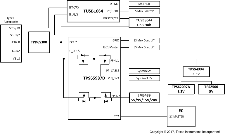
GUID-331AEBCE-C877-48B3-8562-8EA145EF0B09-low.gif Figure 9-9 USB and DisplayPort Dock Block Diagram