JAJSHC5B May 2019 – October 2022 TPS65987DDJ
PRODUCTION DATA
- 1 特長
- 2 アプリケーション
- 3 概要
- 4 Revision History
- 5 Pin Configuration and Functions
-
6 Specifications
- 6.1 Absolute Maximum Ratings
- 6.2 ESD Ratings
- 6.3 Recommended Operating Conditions
- 6.4 Thermal Information
- 6.5 Power Supply Requirements and Characteristics
- 6.6 Power Consumption Characteristics
- 6.7 Power Switch Characteristics
- 6.8 Cable Detection Characteristics
- 6.9 USB-PD Baseband Signal Requirements and Characteristics
- 6.10 BC1.2 Characteristics
- 6.11 Thermal Shutdown Characteristics
- 6.12 Oscillator Characteristics
- 6.13 I/O Characteristics
- 6.14 I2C Requirements and Characteristics
- 6.15 SPI Controller Timing Requirements
- 6.16 HPD Timing Requirements
- 6.17 Typical Characteristics
- 7 Parameter Measurement Information
-
8 Detailed Description
- 8.1 Overview
- 8.2 Functional Block Diagram
- 8.3
Feature Description
- 8.3.1 USB-PD Physical Layer
- 8.3.2 Power Management
- 8.3.3 Port Power Switches
- 8.3.4 Cable Plug and Orientation Detection
- 8.3.5 Dead Battery Operation
- 8.3.6 Battery Charger Detection and Advertisement
- 8.3.7 ADC
- 8.3.8 DisplayPort HPD
- 8.3.9 Digital Interfaces
- 8.3.10 Digital Core
- 8.3.11 I2C Interfaces
- 8.3.12 SPI Controller Interface
- 8.3.13 Thermal Shutdown
- 8.3.14 Oscillators
- 8.4 Device Functional Modes
-
9 Application and Implementation
- 9.1 Application Information
- 9.2
Typical Applications
- 9.2.1 Type-C VBUS Design Considerations
- 9.2.2 Notebook Design Supporting PD Charging
- 10Power Supply Recommendations
- 11Layout
- 12Device and Documentation Support
- 13Mechanical, Packaging, and Orderable Information
11.7 USB2 Recommended Routing For BC1.2 Detection/Advertisement
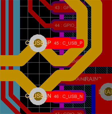
When routing the USB2 signals to the TPS65987DDJ BC1.2 detection pins it is recommended to reduce the amount of excess trace to get to the TPS65987DDJ pins, as this will cause antennae and degrade signal integrity. The USB top/bottom signals are shorted together in this example and the same approach can be used if an external USB mux is used. There are several approaches that can be used to get optimal routing; “tap” the USB2 signals with vias that connect the TPS65987DDJ pins, via up to the layer where the pins are located and continue to route on that layer, or a combination of both.
In this layout example, the D+/D- lines are routed to an internal layer from the connector. They are then via’d up to the TPS65987DDJ directly at the pins. There is a small trace that is connecting the via to the pin on the top layer. When routing the D+/D- in this manner, the added stub is minimal.
 Figure 11-15 Via Connection for USB2
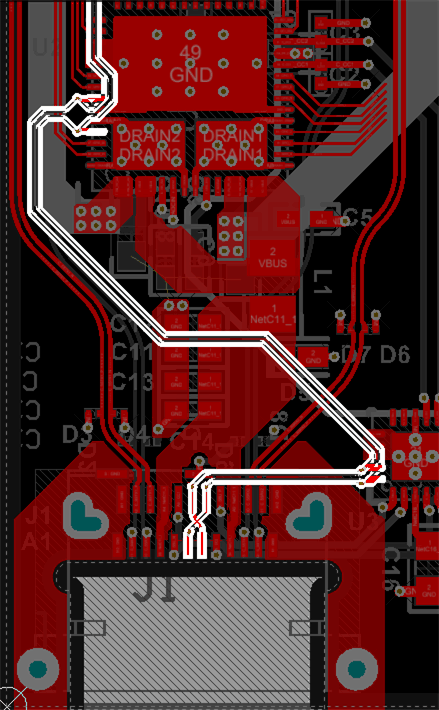
Figure 11-16 shows the entire routing from the Type-C connector, ESD Protection, and TPS65987DDJ BC1.2 Detection. This example does not take length matching into consideration but it is recommended to follow standard USB2 rules for routing and length matching.
 Figure 11-16 Complete USB2 Routing