JAJSJT6A August   2020  – July 2021 TPS65994AD

PRODUCTION DATA  

  1. 特長
  2. アプリケーション
  3. 概要
  4. Revision History
  5. Pin Configuration and Functions
  6. Specifications
    1. 6.1  Absolute Maximum Ratings
    2. 6.2  ESD Ratings
    3. 6.3  Recommended Operating Conditions
    4. 6.4  Recommended Capacitance
    5. 6.5  Thermal Information
    6. 6.6  Power Supply Characteristics
    7. 6.7  Power Consumption
    8. 6.8  PP_5V Power Switch Characteristics
    9. 6.9  PP_EXT Power Switch Characteristics
    10. 6.10 Power Path Supervisory
    11. 6.11 CC Cable Detection Parameters
    12. 6.12 CC VCONN Parameters
    13. 6.13 CC PHY Parameters
    14. 6.14 Thermal Shutdown Characteristics
    15. 6.15 ADC Characteristics
    16. 6.16 Input/Output (I/O) Characteristics
    17. 6.17 I2C Requirements and Characteristics
    18. 6.18 Typical Characteristics
  7. Parameter Measurement Information
  8. Detailed Description
    1. 8.1 Overview
    2. 8.2 Functional Block Diagram
    3. 8.3 Feature Description
      1. 8.3.1  USB-PD Physical Layer
        1. 8.3.1.1 USB-PD Encoding and Signaling
        2. 8.3.1.2 USB-PD Bi-Phase Marked Coding
        3. 8.3.1.3 USB-PD Transmit (TX) and Receive (Rx) Masks
        4. 8.3.1.4 USB-PD BMC Transmitter
        5. 8.3.1.5 USB-PD BMC Receiver
        6. 8.3.1.6 Squelch Receiver
      2. 8.3.2  Power Management
        1. 8.3.2.1 Power-On And Supervisory Functions
        2. 8.3.2.2 VBUS LDO
      3. 8.3.3  Power Paths
        1. 8.3.3.1 Internal Sourcing Power Paths
          1. 8.3.3.1.1  PP_5Vx Current Clamping
          2. 8.3.3.1.2  PP_5Vx Local Overtemperature Shut Down (OTSD)
          3. 8.3.3.1.3  PP_5Vx Current Sense
          4. 8.3.3.1.4  PP_5Vx OVP
          5. 8.3.3.1.5  PP_5Vx UVLO
          6. 8.3.3.1.6  PP_5Vx Reverse Current Protection
          7. 8.3.3.1.7  Fast Role Swap
          8. 8.3.3.1.8  PP_CABLE Current Clamp
          9. 8.3.3.1.9  PP_CABLE Local Overtemperature Shut Down (OTSD)
          10. 8.3.3.1.10 PP_CABLE UVLO
        2. 8.3.3.2 Sink Path Control
          1. 8.3.3.2.1 Overvoltage Protection (OVP)
          2. 8.3.3.2.2 Reverse-Current Protection (RCP)
          3. 8.3.3.2.3 VBUS UVLO
          4. 8.3.3.2.4 Discharging VBUS to Safe Voltage
      4. 8.3.4  Cable Plug and Orientation Detection
        1. 8.3.4.1 Configured as a Source
        2. 8.3.4.2 Configured as a Sink
        3. 8.3.4.3 Configured as a DRP
        4. 8.3.4.4 Fast Role Swap Signal Detection
        5. 8.3.4.5 Dead Battery Advertisement
      5. 8.3.5  Default Behavior Configuration (ADCIN1, ADCIN2)
      6. 8.3.6  ADC
      7. 8.3.7  DisplayPort Hot-Plug Detect (HPD)
      8. 8.3.8  Digital Interfaces
        1. 8.3.8.1 General GPIO
        2. 8.3.8.2 I2C Interface
      9. 8.3.9  Digital Core
      10. 8.3.10 I2C Interface
        1. 8.3.10.1 I2C Interface Description
        2. 8.3.10.2 I2C Clock Stretching
        3. 8.3.10.3 I2C Address Setting
        4. 8.3.10.4 Unique Address Interface
    4. 8.4 Device Functional Modes
      1. 8.4.1 Pin Strapping to Configure Default Behavior
      2. 8.4.2 Power States
      3. 8.4.3 Thermal Shutdown
  9. Application and Implementation
    1. 9.1 Application Information
    2. 9.2 Typical Application
      1. 9.2.1 Type-C VBUS Design Considerations
        1. 9.2.1.1 Design Requirements
        2. 9.2.1.2 Detailed Design Procedure
          1. 9.2.1.2.1 Type-C Connector VBUS Capacitors
          2. 9.2.1.2.2 VBUS Schottky and TVS Diodes
        3. 9.2.1.3 Application Curves
      2. 9.2.2 Notebook Design Supporting PD Charging
        1. 9.2.2.1 USB and DisplayPort Notebook Supporting PD Charging
          1. 9.2.2.1.1 Design Requirements
          2. 9.2.2.1.2 Detailed Design Procedure
            1. 9.2.2.1.2.1 USB Power Delivery Source Capabilities
            2. 9.2.2.1.2.2 USB Power Delivery Sink Capabilities
            3. 9.2.2.1.2.3 USB and DisplayPort Supported Data Modes
            4. 9.2.2.1.2.4 TUSB1046 Super Speed Mux GPIO Control
        2. 9.2.2.2 Thunderbolt Notebook Supporting PD Charging
          1. 9.2.2.2.1 Design Requirements
          2. 9.2.2.2.2 Detailed Design Procedure
            1. 9.2.2.2.2.1 USB Power Delivery Source Capabilities
            2. 9.2.2.2.2.2 USB Power Delivery Sink Capabilities
            3. 9.2.2.2.2.3 Thunderbolt Supported Data Modes
            4. 9.2.2.2.2.4 I2C Design Requirements
            5. 9.2.2.2.2.5 TS3DS10224 SBU Mux for AUX and LSTX/RX
  10. 10Power Supply Recommendations
    1. 10.1 3.3-V Power
      1. 10.1.1 VIN_3V3 Input Switch
      2. 10.1.2 VBUS 3.3-V LDO
    2. 10.2 1.5-V Power
    3. 10.3 Recommended Supply Load Capacitance
  11. 11Layout
    1. 11.1 Layout Guidelines
      1. 11.1.1 Top TPS65994AD Placement and Bottom Component Placement and Layout
    2. 11.2 Layout Example
    3. 11.3 Component Placement
    4. 11.4 Routing PP_5V, VBUS, VIN_3V3, LDO_3V3, LDO_1V5
    5. 11.5 Routing CC and GPIO
  12. 12Device and Documentation Support
    1. 12.1 Device Support
      1. 12.1.1 Third-Party Products Disclaimer
    2. 12.2 Documentation Support
      1. 12.2.1 Related Documentation
    3. 12.3 サポート・リソース
    4. 12.4 Trademarks
    5. 12.5 Electrostatic Discharge Caution
    6. 12.6 Glossary
  13. 13Mechanical, Packaging, and Orderable Information
    1. 13.1 Package Option Addendum
      1. 13.1.1 Tape and Reel Information

パッケージ・オプション

メカニカル・データ(パッケージ|ピン)
サーマルパッド・メカニカル・データ
発注情報
Overvoltage Protection (OVP)

The application firmware enables the OVP and configures it based on the expected Px_VBUS voltage. If the voltage on Px_VBUS surpasses the configured threshold VOVP4VSYS = VOVP4RCP/rOVP, then Px_GATE_VSYS is automatically disabled within tPx_GATE_VSYS_FSD to protect the system. If the voltage on Px_VBUS surpasses the configured threshold VOVP4RCP then Px_GATE_VBUS is automatically disabled within tPx_GATE_VBUS_OVP. When VPx_VBUS falls below VOVP4RCP - VOVP4RCPH Px_GATE_VBUS is automatically re-enabled within
tPx_GATE_VBUS_ON since the OVP condition has cleared.
This allows two sinking power paths to be enabled simultaneously and Px_GATE_VBUS will be disabled when necessary to ensure that VPx_VBUS remains below VOVP4RCP.

While the TPS65994AD is in the BOOT mode in a dead-battery scenario (that is VIN_3V3 is low) it handles an OVP condition slightly differently. As long as the OVP condition is present Px_GATE_VBUS and Px_GATE_VSYS are disabled. Once the OVP condition clears, both Px_GATE_VBUS and Px_GATE_VSYS are re-enabled (unless ADCINx are configured in SafeMode). Since this is a dead-battery condition, the TPS65994AD will be drawing approximately IVIN_3V3,ActSnk from PA_VBUS or PB_VBUS during this time to help discharge it.
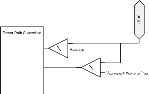
GUID-E9714F34-127C-43A3-80E8-55CD543330E0-low.gif Figure 8-13 Diagram for OVP Comparators