JAJSJT6A August   2020  – July 2021 TPS65994AD

PRODUCTION DATA  

  1. 特長
  2. アプリケーション
  3. 概要
  4. Revision History
  5. Pin Configuration and Functions
  6. Specifications
    1. 6.1  Absolute Maximum Ratings
    2. 6.2  ESD Ratings
    3. 6.3  Recommended Operating Conditions
    4. 6.4  Recommended Capacitance
    5. 6.5  Thermal Information
    6. 6.6  Power Supply Characteristics
    7. 6.7  Power Consumption
    8. 6.8  PP_5V Power Switch Characteristics
    9. 6.9  PP_EXT Power Switch Characteristics
    10. 6.10 Power Path Supervisory
    11. 6.11 CC Cable Detection Parameters
    12. 6.12 CC VCONN Parameters
    13. 6.13 CC PHY Parameters
    14. 6.14 Thermal Shutdown Characteristics
    15. 6.15 ADC Characteristics
    16. 6.16 Input/Output (I/O) Characteristics
    17. 6.17 I2C Requirements and Characteristics
    18. 6.18 Typical Characteristics
  7. Parameter Measurement Information
  8. Detailed Description
    1. 8.1 Overview
    2. 8.2 Functional Block Diagram
    3. 8.3 Feature Description
      1. 8.3.1  USB-PD Physical Layer
        1. 8.3.1.1 USB-PD Encoding and Signaling
        2. 8.3.1.2 USB-PD Bi-Phase Marked Coding
        3. 8.3.1.3 USB-PD Transmit (TX) and Receive (Rx) Masks
        4. 8.3.1.4 USB-PD BMC Transmitter
        5. 8.3.1.5 USB-PD BMC Receiver
        6. 8.3.1.6 Squelch Receiver
      2. 8.3.2  Power Management
        1. 8.3.2.1 Power-On And Supervisory Functions
        2. 8.3.2.2 VBUS LDO
      3. 8.3.3  Power Paths
        1. 8.3.3.1 Internal Sourcing Power Paths
          1. 8.3.3.1.1  PP_5Vx Current Clamping
          2. 8.3.3.1.2  PP_5Vx Local Overtemperature Shut Down (OTSD)
          3. 8.3.3.1.3  PP_5Vx Current Sense
          4. 8.3.3.1.4  PP_5Vx OVP
          5. 8.3.3.1.5  PP_5Vx UVLO
          6. 8.3.3.1.6  PP_5Vx Reverse Current Protection
          7. 8.3.3.1.7  Fast Role Swap
          8. 8.3.3.1.8  PP_CABLE Current Clamp
          9. 8.3.3.1.9  PP_CABLE Local Overtemperature Shut Down (OTSD)
          10. 8.3.3.1.10 PP_CABLE UVLO
        2. 8.3.3.2 Sink Path Control
          1. 8.3.3.2.1 Overvoltage Protection (OVP)
          2. 8.3.3.2.2 Reverse-Current Protection (RCP)
          3. 8.3.3.2.3 VBUS UVLO
          4. 8.3.3.2.4 Discharging VBUS to Safe Voltage
      4. 8.3.4  Cable Plug and Orientation Detection
        1. 8.3.4.1 Configured as a Source
        2. 8.3.4.2 Configured as a Sink
        3. 8.3.4.3 Configured as a DRP
        4. 8.3.4.4 Fast Role Swap Signal Detection
        5. 8.3.4.5 Dead Battery Advertisement
      5. 8.3.5  Default Behavior Configuration (ADCIN1, ADCIN2)
      6. 8.3.6  ADC
      7. 8.3.7  DisplayPort Hot-Plug Detect (HPD)
      8. 8.3.8  Digital Interfaces
        1. 8.3.8.1 General GPIO
        2. 8.3.8.2 I2C Interface
      9. 8.3.9  Digital Core
      10. 8.3.10 I2C Interface
        1. 8.3.10.1 I2C Interface Description
        2. 8.3.10.2 I2C Clock Stretching
        3. 8.3.10.3 I2C Address Setting
        4. 8.3.10.4 Unique Address Interface
    4. 8.4 Device Functional Modes
      1. 8.4.1 Pin Strapping to Configure Default Behavior
      2. 8.4.2 Power States
      3. 8.4.3 Thermal Shutdown
  9. Application and Implementation
    1. 9.1 Application Information
    2. 9.2 Typical Application
      1. 9.2.1 Type-C VBUS Design Considerations
        1. 9.2.1.1 Design Requirements
        2. 9.2.1.2 Detailed Design Procedure
          1. 9.2.1.2.1 Type-C Connector VBUS Capacitors
          2. 9.2.1.2.2 VBUS Schottky and TVS Diodes
        3. 9.2.1.3 Application Curves
      2. 9.2.2 Notebook Design Supporting PD Charging
        1. 9.2.2.1 USB and DisplayPort Notebook Supporting PD Charging
          1. 9.2.2.1.1 Design Requirements
          2. 9.2.2.1.2 Detailed Design Procedure
            1. 9.2.2.1.2.1 USB Power Delivery Source Capabilities
            2. 9.2.2.1.2.2 USB Power Delivery Sink Capabilities
            3. 9.2.2.1.2.3 USB and DisplayPort Supported Data Modes
            4. 9.2.2.1.2.4 TUSB1046 Super Speed Mux GPIO Control
        2. 9.2.2.2 Thunderbolt Notebook Supporting PD Charging
          1. 9.2.2.2.1 Design Requirements
          2. 9.2.2.2.2 Detailed Design Procedure
            1. 9.2.2.2.2.1 USB Power Delivery Source Capabilities
            2. 9.2.2.2.2.2 USB Power Delivery Sink Capabilities
            3. 9.2.2.2.2.3 Thunderbolt Supported Data Modes
            4. 9.2.2.2.2.4 I2C Design Requirements
            5. 9.2.2.2.2.5 TS3DS10224 SBU Mux for AUX and LSTX/RX
  10. 10Power Supply Recommendations
    1. 10.1 3.3-V Power
      1. 10.1.1 VIN_3V3 Input Switch
      2. 10.1.2 VBUS 3.3-V LDO
    2. 10.2 1.5-V Power
    3. 10.3 Recommended Supply Load Capacitance
  11. 11Layout
    1. 11.1 Layout Guidelines
      1. 11.1.1 Top TPS65994AD Placement and Bottom Component Placement and Layout
    2. 11.2 Layout Example
    3. 11.3 Component Placement
    4. 11.4 Routing PP_5V, VBUS, VIN_3V3, LDO_3V3, LDO_1V5
    5. 11.5 Routing CC and GPIO
  12. 12Device and Documentation Support
    1. 12.1 Device Support
      1. 12.1.1 Third-Party Products Disclaimer
    2. 12.2 Documentation Support
      1. 12.2.1 Related Documentation
    3. 12.3 サポート・リソース
    4. 12.4 Trademarks
    5. 12.5 Electrostatic Discharge Caution
    6. 12.6 Glossary
  13. 13Mechanical, Packaging, and Orderable Information
    1. 13.1 Package Option Addendum
      1. 13.1.1 Tape and Reel Information

パッケージ・オプション

メカニカル・データ(パッケージ|ピン)
サーマルパッド・メカニカル・データ
発注情報

Component Placement

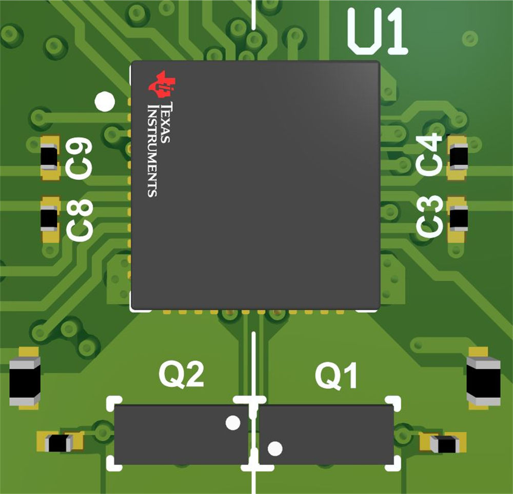
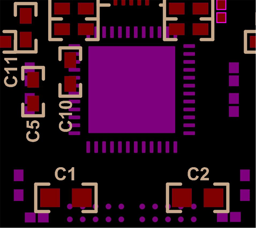
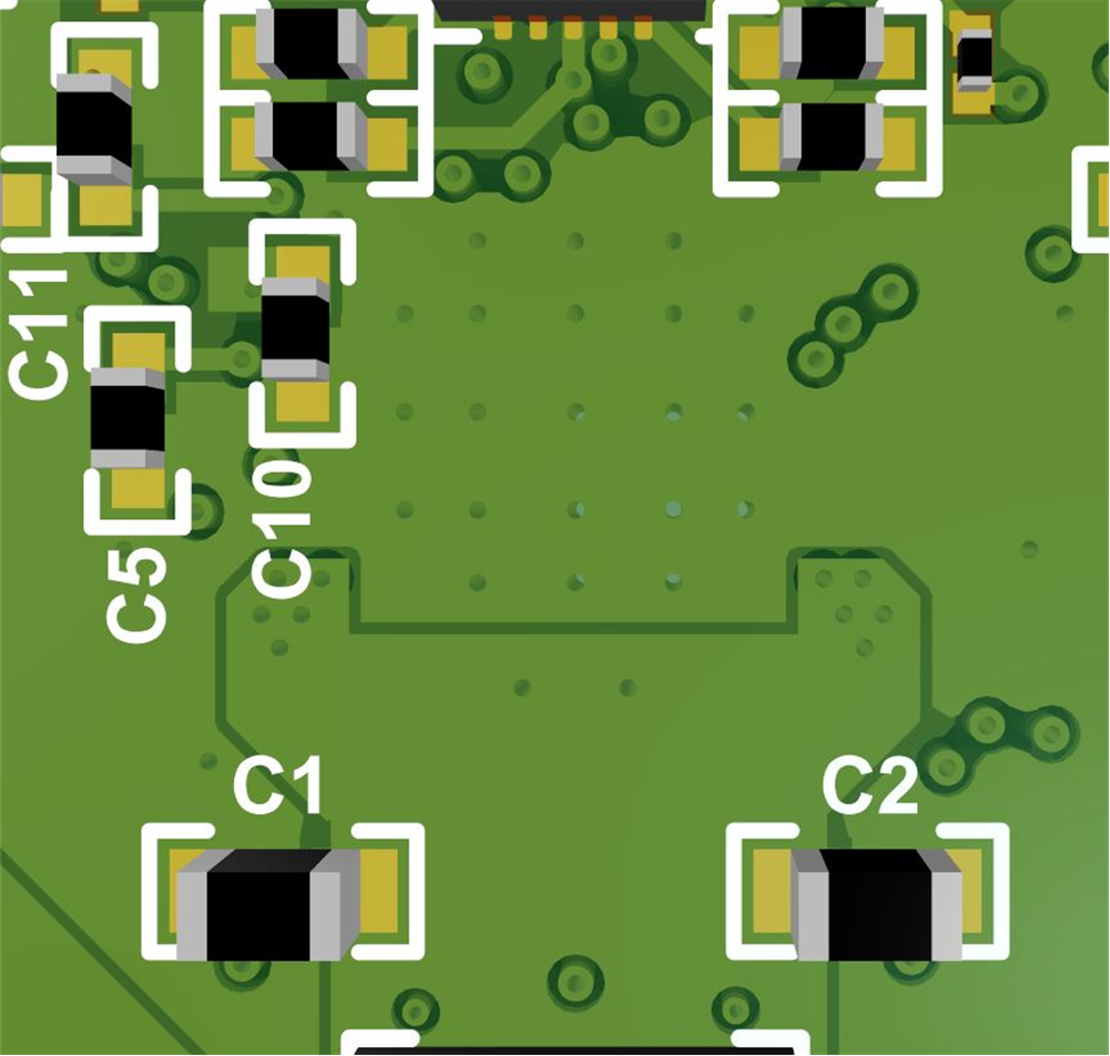
Top and bottom placement is used for this example to minimize solution size. The TPS65994AD is placed on the top side of the board and the majority of its components are placed on the bottom side. When placing the components on the bottom side, it is recommended that they are placed directly under the TPS65994AD. When placing the VBUS and PPHV capacitors it is easiest to place them with the GND terminal of the capacitors to face outward from the TPS65994AD or to the side since the drain connection pads on the bottom layer should not be connected to anything and left floating. All other components that are for pins on the GND pad side of the TPS65994AD should be placed where the GND terminal is underneath the GND pad.

The CC capacitors should be placed on the same side as the TPS65994AD close to the respective CC1 and CC2 pins. Do NOT via to another layer in between the CC pins to the CC capacitor, placing a via after the CC capacitor is recommended.

The ADCIN1/2 voltage divider resistors can be placed where convenient. In this layout example they are placed on the opposite layer of the TPS65994AD close to the LDO_3V3 pin to simplify routing.

The figures below show the placement in 2-D and 3-D.
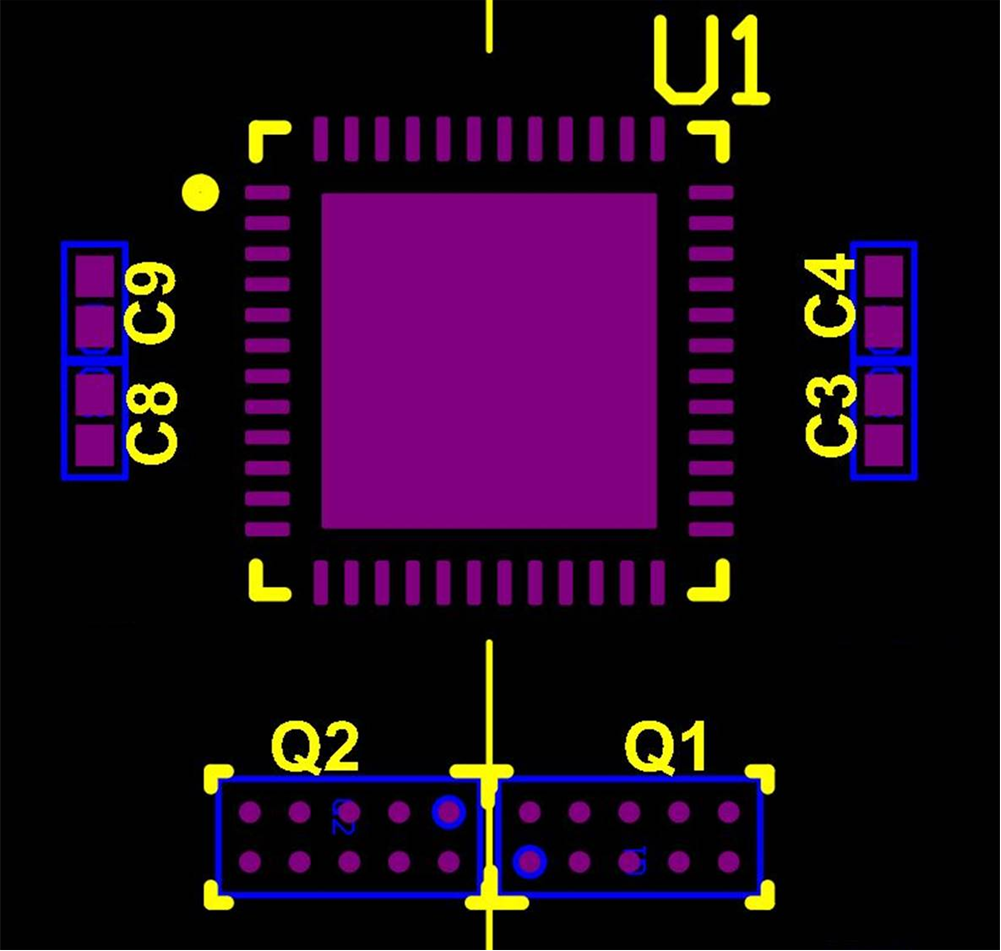
GUID-20200625-SS0I-JTJR-LD3M-G2NDBPSCSCSC-low.pngFigure 11-2 Top View Layout
GUID-20200625-SS0I-H1QD-VGFD-DF9XXL7PLNL5-low.pngFigure 11-4 Top View 3-D
GUID-20200625-SS0I-T1NM-8LTJ-JZ6LC8TDPSZ0-low.pngFigure 11-3 Bottom View Layout (Flipped)
GUID-20200625-SS0I-TGTM-B0NC-SWMGKKS1XSQL-low.pngFigure 11-5 Bottom View 3-D