JAJSHS4B August 2019 – December 2019 TPS66020 , TPS66021
PRODUCTION DATA.
- 1 特長
- 2 アプリケーション
- 3 概要
- 4 改訂履歴
- 5 Pin Configuration and Functions
-
6 Specifications
- 6.1 Absolute Maximum Ratings
- 6.2 ESD Ratings
- 6.3 Recommended Operating Conditions
- 6.4 Recommended Supply Load Capacitance
- 6.5 Thermal Information
- 6.6 PP5V Power Switch Characteristics
- 6.7 PPHV Power Switch Characteristics
- 6.8 Power Path Supervisory
- 6.9 VBUS LDO Characteristics
- 6.10 Thermal Shutdown Characteristics
- 6.11 Input-output (I/O) Characteristics
- 6.12 Power Consumption Characteristics
- 6.13 Typical Characteristics
- 7 Parameter Measurement Information
-
8 Detailed Description
- 8.1 Overview
- 8.2 Functional Block Diagram
- 8.3 Feature Description
- 8.4 Device Functional Modes
-
9 Application and Implementation
- 9.1 Application Information
- 9.2
Typical Application
- 9.2.1 Design Requirements
- 9.2.2
Detailed Design Procedure
- 9.2.2.1 External Current Reference Resistor (RIREF)
- 9.2.2.2 External VLDO Capacitor (CVLDO)
- 9.2.2.3 PP5V Power Path Capacitance
- 9.2.2.4 PPHV, VBUS Power Path Capacitance
- 9.2.2.5 VBUS TVS Protection (Optional)
- 9.2.2.6 VBUS Schottky Diode Protection (Optional)
- 9.2.2.7 VBUS Overvoltage Protection (Optional)
- 9.2.2.8 Dead Battery Support
- 9.2.2.9 Fast Role Swap (FRS) (Optional)
- 9.2.3 Application Curves
- 10Power Supply Recommendations
- 11Layout
- 12デバイスおよびドキュメントのサポート
- 13メカニカル、パッケージ、および注文情報
6.13 Typical Characteristics
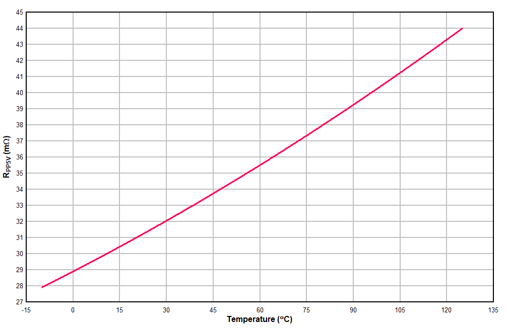 Figure 1. RPP5V versus Temperature
 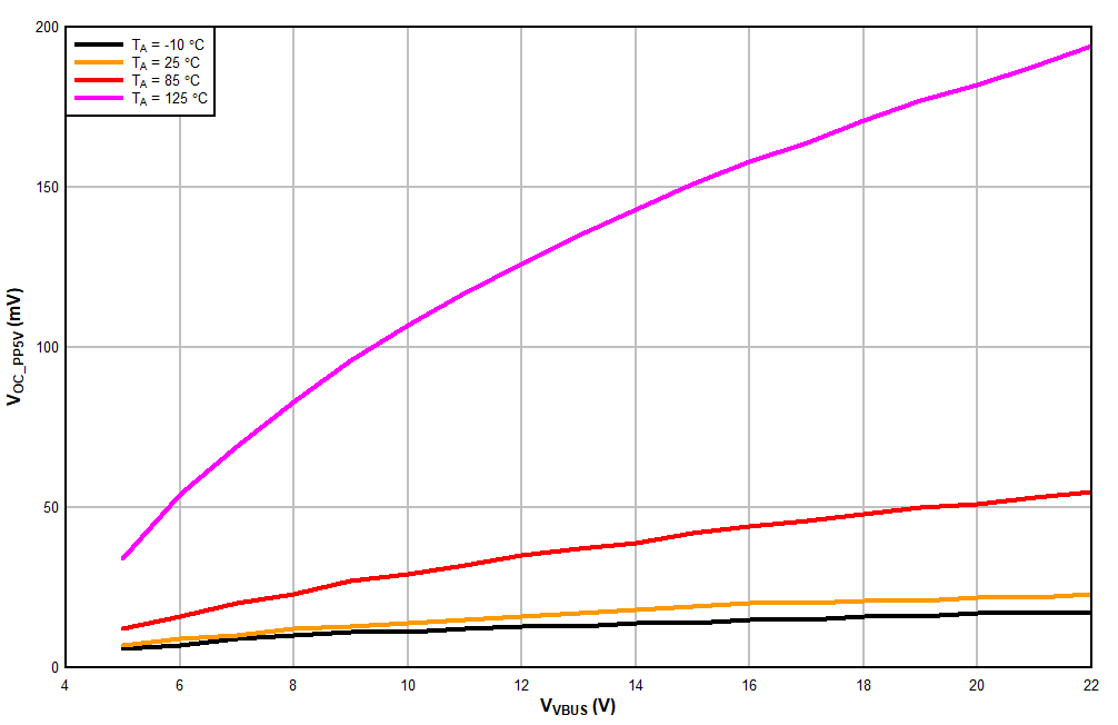 Figure 3. VOC_PP5V, PP5V Open Circuit Voltage versus VBUS
 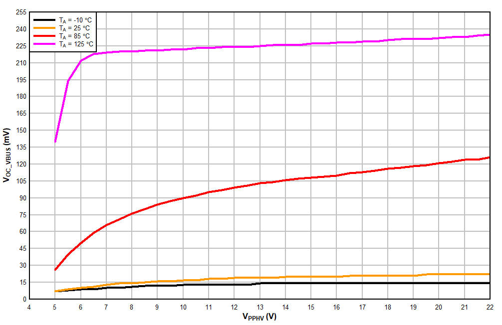 Figure 5. VOC_VBUS, VBUS Open Circuit Voltage versus PPHV
 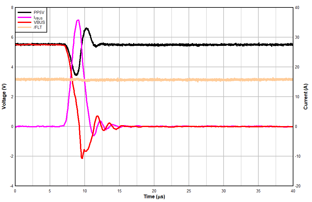 Figure 7. PP5V Current Limit (3 A) Response with Short (Zoomed In At Time of Short)
  Figure 9. VBUS OVP Response with 6-V Threshold
 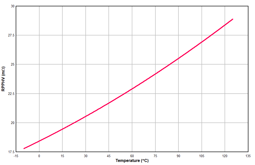 Figure 2. RPPHV versus Temperature
 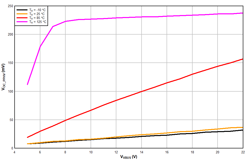 Figure 4. VOC_PPHV, PPHV Open Circuit Voltage versus VBUS
  Figure 6. PP5V Current Limit (3 A) Response with Short (Zoomed Out)
  Figure 8. PP5V Current Limit (3 A) Response with Persistent Short Showing TSD Protection and Recovery