JAJSFL1C December   2013  – June 2018 TPS709-Q1

PRODUCTION DATA.  

  1. 特長
  2. アプリケーション
  3. 概要
    1.     Device Images
      1.      代表的なアプリケーション回路
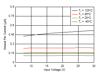
      2.      GND電流とVINおよび温度との関係
  4. 改訂履歴
  5. Pin Configuration and Functions
    1.     Pin Functions
  6. Specifications
    1. 6.1 Absolute Maximum Ratings
    2. 6.2 ESD Ratings
    3. 6.3 Recommended Operating Conditions
    4. 6.4 Thermal Information
    5. 6.5 Electrical Characteristics
    6. 6.6 Timing Requirements
    7. 6.7 Typical Characteristics
  7. Detailed Description
    1. 7.1 Overview
    2. 7.2 Functional Block Diagram
    3. 7.3 Feature Description
      1. 7.3.1 Undervoltage Lockout (UVLO)
      2. 7.3.2 Shutdown
      3. 7.3.3 Reverse Current Protection
      4. 7.3.4 Internal Current Limit
      5. 7.3.5 Thermal Protection
    4. 7.4 Device Functional Modes
      1. 7.4.1 Normal Operation
      2. 7.4.2 Dropout Operation
      3. 7.4.3 Disabled
  8. Application and Implementation
    1. 8.1 Application Information
      1. 8.1.1 Input and Output Capacitor Considerations
      2. 8.1.2 Dropout Voltage
      3. 8.1.3 Transient Response
    2. 8.2 Typical Application
      1. 8.2.1 Design Requirements
      2. 8.2.2 Detailed Design Procedure
      3. 8.2.3 Application Curves
  9. Power Supply Recommendations
  10. 10Layout
    1. 10.1 Layout Guidelines
      1. 10.1.1 Board Layout Recommendations to Improve PSRR and Noise Performance
      2. 10.1.2 Power Dissipation
    2. 10.2 Layout Examples
  11. 11デバイスおよびドキュメントのサポート
    1. 11.1 デバイス・サポート
      1. 11.1.1 開発サポート
        1. 11.1.1.1 評価モジュール
        2. 11.1.1.2 SPICEモデル
      2. 11.1.2 デバイスの項目表記
    2. 11.2 ドキュメントのサポート
      1. 11.2.1 関連資料
    3. 11.3 ドキュメントの更新通知を受け取る方法
    4. 11.4 コミュニティ・リソース
    5. 11.5 商標
    6. 11.6 静電気放電に関する注意事項
    7. 11.7 Glossary
  12. 12メカニカル、パッケージ、および注文情報

パッケージ・オプション

デバイスごとのパッケージ図は、PDF版データシートをご参照ください。

メカニカル・データ(パッケージ|ピン)
  • DBV|5
  • DRV|6
サーマルパッド・メカニカル・データ
発注情報

Typical Characteristics

Over operating temperature range (TJ = –40°C to 125°C), IOUT = 10 mA, VEN = 2 V, COUT = 2.2 μF, and VIN = VOUT(nom) + 1 V or 2.7 V (whichever is greater), unless otherwise noted. Typical values are at TJ = 25°C.
TPS709-Q1 D001_SLVSCE6.gif
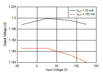
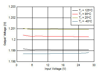
Figure 1. 1.2-V Line Regulation vs VIN and Temperature
TPS709-Q1 D003_SLVSCE6.gif
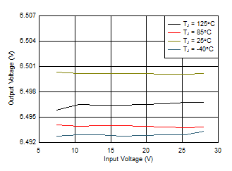
Figure 3. 6.5-V Line Regulation vs VIN and Temperature
TPS709-Q1 D005_SLVSCE6.gif
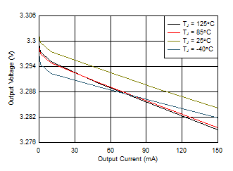
Figure 5. 3.3-V Load Regulation vs IOUT and Temperature
TPS709-Q1 D007_SLVSCE6.gif
Figure 7. 1.2-V Output Voltage vs Temperature
TPS709-Q1 D009_SLVSCE6.gif
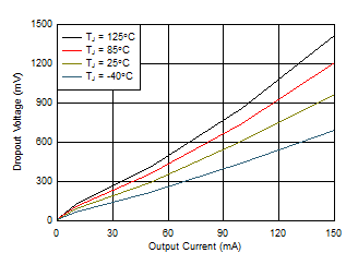
Figure 9. 3.3-V Dropout Voltage vs IOUT and Temperature
TPS709-Q1 D011_SLVSCE6.gif
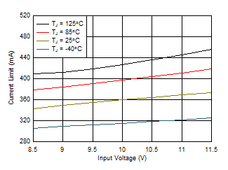
Figure 11. 1.2-V Current Limit vs VIN and Temperature
TPS709-Q1 D013_SLVSCE6.gif
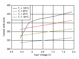
Figure 13. 6.5-V Current Limit vs VIN and Temperature
TPS709-Q1 D015_SLVSCE6.gif
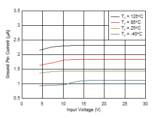
Figure 15. 3.3-V Ground Pin Current vs VIN and
Temperature
TPS709-Q1 D017_SLVSCE6.gif
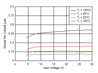
Figure 17. 3.3-V Ground Current vs VIN and
Temperature with EN Floating
TPS709-Q1 D019_SLVSCE6.gif
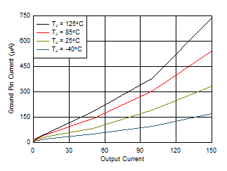
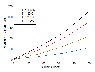
Figure 19. 3.3-V Ground Pin Current vs IOUT and
Temperature
TPS709-Q1 D021_SLVSCE6.gif
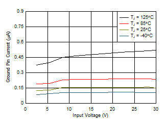
Figure 21. 1.2-V Shutdown Current vs VIN and Temperature
TPS709-Q1 D023_SLVSCE6.gif
Figure 23. 6.5-V Shutdown Current vs VIN and Temperature
TPS709-Q1 D002_SBVS245.gif
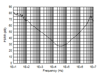
Figure 25. Power-Supply Rejection Ratio vs Frequency
TPS709-Q1 G020_BVS245.gif
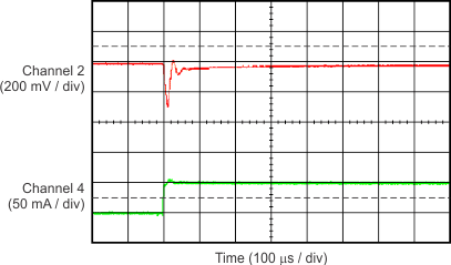
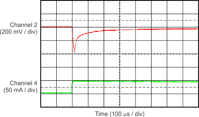
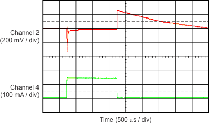
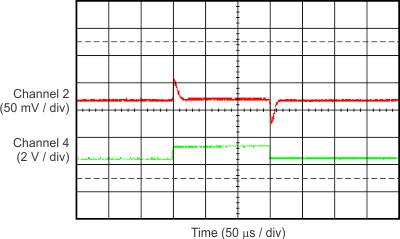
Channel 2 = VOUT, channel 4 = IOUT, VIN = 2.7 V
Figure 27. TPS70912-Q1 Load Transient (0 mA to 50 mA)
TPS709-Q1 G022_BVS245.gif
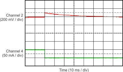
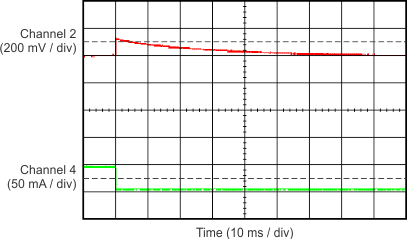
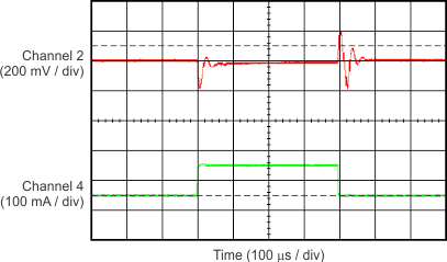
Channel 2 = VOUT, channel 4 = IOUT, VIN = 2.7 V
Figure 29. TPS70912-Q1 Load Transient (50 mA to 0 mA)
TPS709-Q1 G024_BVS245.gif
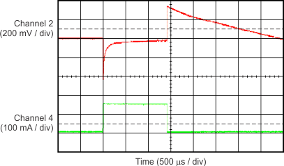
Channel 2 = VOUT, channel 4 = IOUT, VIN = 4.3 V
Figure 31. TPS70933-Q1 Load Transient (0 mA to 50 mA)
TPS709-Q1 G026_BVS245.gif
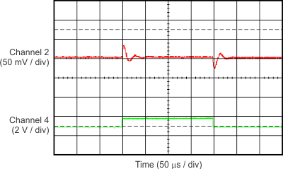
Channel 2 = VOUT, channel 4 = IOUT, VIN = 4.3 V
Figure 33. TPS70933-Q1 Load Transient (50 mA to 0 mA)
TPS709-Q1 G028_BVS245.gif
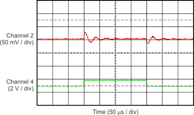
Channel 2 = VOUT, channel 4 = VIN, IOUT = 10 mA
Figure 35. TPS70912-Q1 Line Transient (2.7 V to 3.7 V)
TPS709-Q1 G030_BVS245.gif
Channel 2 = VOUT, channel 4 = VIN, IOUT = 10 mA
Figure 37. TPS70933-Q1 Line Transient (4.3 V to 5.3 V)
TPS709-Q1 G032_BVS245.gif
Channel 1 = EN, channel 2 = VOUT, VIN = 4.3 V, COUT = 2.2 µF, TPS70633
Figure 39. Power-Up with Enable
TPS709-Q1 G034_BVS245.gif
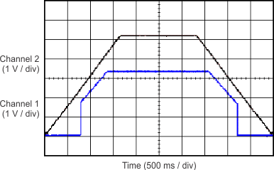
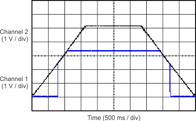
Channel 1 = VIN, channel 2 = VOUT, IOUT = 150 mA, TPS70633
Figure 41. Power-Up and Power-Down Response
TPS709-Q1 D002_SLVSCE6.gif
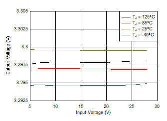
Figure 2. 3.3-V Line Regulation vs VIN and Temperature
TPS709-Q1 D004_SLVSCE6.gif
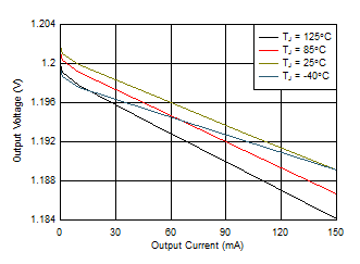
Figure 4. 1.2-V Load Regulation vs IOUT and Temperature
TPS709-Q1 D006_SLVSCE6.gif
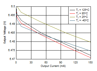
Figure 6. 6.5-V Load Regulation vs IOUT and Temperature
TPS709-Q1 D008_SLVSCE6.gif
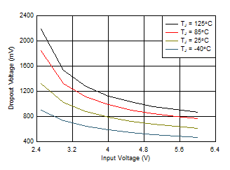
Figure 8. 6.5-V Dropout Voltage vs VIN and Temperature
TPS709-Q1 D010_SLVSCE6.gif
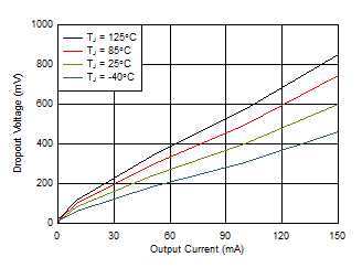
Figure 10. Dropout Voltage vs IOUT and Temperature
TPS709-Q1 D012_SLVSCE6.gif
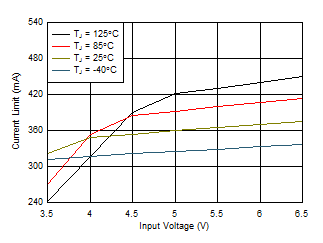
Figure 12. 3.3-V Current Limit vs VIN and Temperature
TPS709-Q1 D014_SLVSCE6.gif
Figure 14. 1.2-V Ground Pin Current vs VIN and
Temperature
TPS709-Q1 D016_SLVSCE6.gif
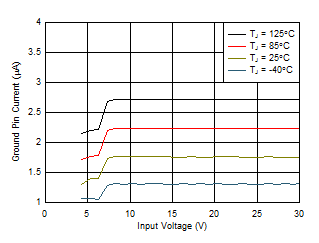
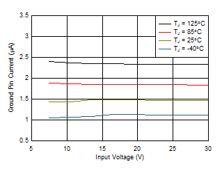
Figure 16. 6.5-V Ground Pin Current vs VIN and
Temperature
TPS709-Q1 D018_SLVSCE6.gif
Figure 18. 1.2-V Ground Pin Current vs IOUT and Temperature
TPS709-Q1 D020_SLVSCE6.gif
Figure 20. 6.5-V Ground Pin Current vs IOUT and Temperature
TPS709-Q1 D022_SLVSCE6.gif
Figure 22. 3.3-V Shutdown Current vs VIN and Temperature
TPS709-Q1 D024_SLVSCE6.gif
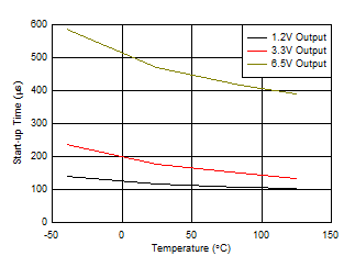
Figure 24. Start-Up Time vs Temperature
TPS709-Q1 D012_SBVS245.gif
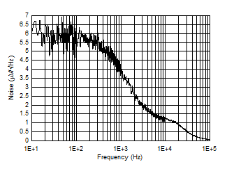
Figure 26. Noise
TPS709-Q1 G021_BVS245.gif
Channel 2 = VOUT, channel 4 = IOUT, VIN = 2.7 V
Figure 28. TPS70912-Q1 Load Transient (1 mA to 150 mA)
TPS709-Q1 G023_BVS245.gif
Channel 2 = VOUT, channel 4 = IOUT, VIN = 2.7 V
Figure 30. TPS70912-Q1 Load Transient (50 mA to 150 mA)
TPS709-Q1 G025_BVS245.gif
Channel 2 = VOUT, channel 4 = IOUT, VIN = 4.3 V
Figure 32. TPS70933-Q1 Load Transient (1 mA to 150 mA)
TPS709-Q1 G027_BVS245.gif
Channel 2 = VOUT, channel 4 = IOUT, VIN = 4.3 V
Figure 34. TPS70933-Q1 Load Transient (50 mA to 150 mA)
TPS709-Q1 G029_BVS245.gif
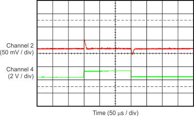
Channel 2 = VOUT, channel 4 = VIN, IOUT = 50 mA
Figure 36. TPS70912-Q1 Line Transient (2.7 V to 3.7 V)
TPS709-Q1 G031_BVS245.gif
Channel 2 = VOUT, channel 4 = VIN, IOUT = 50 mA
Figure 38. TPS70933-Q1 Line Transient (4.3 V to 5.3 V)
TPS709-Q1 G033_BVS245.gif
Channel 1 = VIN, channel 2 = VOUT, IOUT = 3 mA, TPS70633
Figure 40. Power-Up and Power-Down Response