JAJS385T May 2001 – December 2022 TPS715
PRODUCTION DATA
- 1 特長
- 2 アプリケーション
- 3 概要
- 4 Revision History
- 5 Pin Configuration and Functions
- 6 Specifications
- 7 Detailed Description
- 8 Application and Implementation
- 9 Device and Documentation Support
- 10Mechanical, Packaging, and Orderable Information
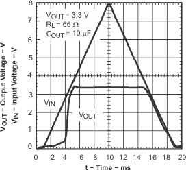
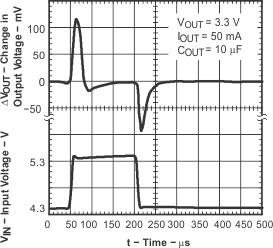
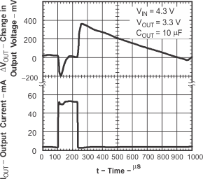
8.2.2 Application Curves
at operating temperature TJ = 25°C, VIN = VOUT(NOM) + 1.0 V or 2.5 V (whichever is greater), IOUT = 1 mA, CIN = 1 µF, and COUT = 1 µF (unless otherwise noted)


