デバイスごとのパッケージ図は、PDF版データシートをご参照ください。
This device is designed to have a fast transient response and be stable with 10 µF low ESR capacitors. This combination provides high performance at a reasonable cost.
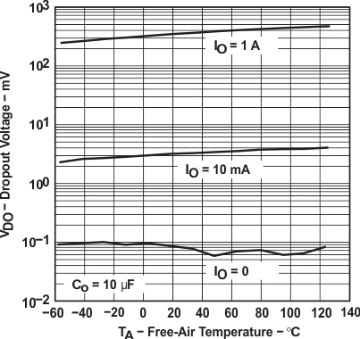
Because the PMOS device behaves as a low-value resistor, the dropout voltage is very low (typically
230 mV at an output current of 1 A for the TPS76750) and is directly proportional to the output current. Additionally, since the PMOS pass element is a voltage-driven device, the quiescent current is very low and independent of output loading (typically
85 µA over the full range of output current, 0 mA to
1 A). These two key specifications yield a significant improvement in operating life for battery-powered systems. This LDO family also features a sleep mode; applying a TTL high signal to EN (enable) shuts down the regulator, reducing the quiescent current to 1 µA at TJ = 25°C.
PART NUMBER | PACKAGE | BODY SIZE (NOM) |
---|---|---|
TPS767xx | SOIC (8) | 4.90 mm × 3.91 mm |
HTSSOP (20) | 6.50 mm x 4.40 mm |
Changes from I Revision (January 2004) to J Revision
The RESET output of the TPS767xx initiates a reset in microcomputer and microprocessor systems in the event of an undervoltage condition. An internal comparator in the TPS767xx monitors the output voltage of the regulator to detect an undervoltage condition on the regulated output voltage.
The TPS767xx is offered in 1.5-V, 1.8-V, 2.5-V, 2.7-V, 2.8-V, 3.0-V, 3.3-V, and 5.0-V fixed-voltage versions and in an adjustable version (programmable over the range of 1.5 V to 5.5 V). Output voltage tolerance is specified as a maximum of 2% over line, load, and temperature ranges. The TPS767xx family is available in 8-pin SOIC and 20-pin PWP packages.
PART NO. (1) | VOLTAGE OPTIONS (V) |
|
---|---|---|
TSSOP (PWP) |
SOIC (D) |
TYP |
TPS76750Q | TPS76750Q | 5 |
TPS76733Q | TPS76733Q | 3.3 |
TPS76730Q | TPS76730Q | 3 |
TPS76728Q | TPS76728Q | 2.8 |
TPS76727Q | TPS76727Q | 2.7 |
TPS76725Q | TPS76725Q | 2.5 |
TPS76718Q | TPS76718Q | 1.8 |
TPS76715Q | TPS76715Q | 1.5 |
TPS76701Q | TPS76701Q | Adjustable 1.5 V to 5.5 V |
PIN | I/O | DESCRIPTION | |
---|---|---|---|
NAME | NO. | ||
SOIC PACKAGE | |||
EN | 2 | I | Enable input |
FB/NC | 7 | I | Feedback input voltage for adjustable device (no connect for fixed options) |
GND | 1 | Regulator ground | |
IN | 3, 4 | I | Input voltage |
OUT | 5, 6 | O | Regulated output voltage |
RESET | 8 | O | RESET output |
HTSSOP PACKAGE | |||
EN | 5 | I | Enable input |
FB/NC | 15 | I | Feedback input voltage for adjustable device (no connect for fixed options) |
GND | 3 | Regulator ground | |
GND/HSINK | 1, 2, 9, 10, 11, 12, 19, 20 | Ground/heatsink | |
IN | 6, 7 | I | Input voltage |
NC | 4, 8, 17, 18 | No connect | |
OUT | 13, 14 | O | Regulated output voltage |
RESET | 16 | O | RESET output |
MIN | MAX | UNIT | ||
---|---|---|---|---|
VI | Input voltage range(2) | –0.3 | 13.5 | V |
Voltage range at EN | –0.3 | VI + 0.3 | V | |
Maximum RESET voltage | 16.5 | |||
Peak output current | Internally limited | |||
VO | Output voltage (OUT, FB) | 7 | V | |
Continuous total power dissipation | See Thermal Information | |||
TJ | Operating junction temperature range | –40 | 125 | °C |
Tstg | Storage temperature range | −65 | 150 | °C |
VALUE | UNIT | |||
---|---|---|---|---|
V(ESD) | Electrostatic discharge | Human body model (HBM), per ANSI/ESDA/JEDEC JS-001, all pins(1) | 2000 | V |
MIN | MAX | UNIT | ||
---|---|---|---|---|
VI(1) | Input voltage | 2.7 | 10 | V |
VO | Output voltage range | 1.2 | 5.5 | V |
IO(2) | Output current | 0 | 1.0 | A |
TJ(2) | Operating junction temperature | –40 | 125 | °C |
THERMAL METRIC(1) | TPS767xxQ | UNIT | ||
---|---|---|---|---|
PWP (HTSSOP) | D (SOIC) | |||
(20 PINS) | (8 PINS) | |||
RθJA | Junction-to-ambient thermal resistance | 35.8 | 106.9 | °C/W |
RθJC(top) | Junction-to-case (top) thermal resistance | 26.1 | 52.5 | °C/W |
RθJB | Junction-to-board thermal resistance | 8.7 | 47.7 | °C/W |
ψJT | Junction-to-top characterization parameter | 0.4 | 9.0 | °C/W |
ψJB | Junction-to-board characterization parameter | 8.6 | 47.1 | °C/W |
RθJC(bot) | Junction-to-case (bottom) thermal resistance | 2.6 | n/a | °C/W |
PARAMETER | TEST CONDITIONS | MIN | TYP | MAX | UNIT | |||
---|---|---|---|---|---|---|---|---|
Output voltage (10 µA to 1 A load) |
TPS76701 | 1.5 V ≤ VO ≤ 5.5 V, | TJ = 25°C | VO | V | |||
1.5 V ≤ VO ≤ 5.5 V, | TJ = −40°C to 125°C | 0.98VO | 1.02VO | |||||
TPS76715 | TJ = 25°C, | 2.7 V < VIN < 10 V | 1.5 | V | ||||
TJ = −40°C to 125°C, | 2.7 V < VIN < 10 V | 1.470 | 1.530 | |||||
TPS76718 | TJ = 25°C, | 2.8 V < VIN < 10 V | 1.8 | V | ||||
TJ = −40°C to 125°C, | 2.8 V < VIN < 10 V | 1.7646 | 1.836 | |||||
TPS76725 | TJ = 25°C, | 3.5 V < VIN < 10 V | 2.5 | V | ||||
TJ = −40°C to 125°C, | 3.5 V < VIN < 10 V | 2.450 | 2.550 | |||||
TPS76727 | TJ = 25°C, | 3.7 V < VIN < 10 V | 2.7 | V | ||||
TJ = −40°C to 125°C, | 3.7 V < VIN < 10 V | 2.646 | 2.754 | |||||
TPS76728 | TJ = 25°C, | 3.8 V < VIN < 10 V | 2.8 | V | ||||
TJ = −40°C to 125°C, | 3.8 V < VIN < 10 V | 2.7446 | 2.856 | |||||
TPS76730 | TJ = 25°C, | 4.0 V < VIN < 10 V | 3 | V | ||||
TJ = −40°C to 125°C, | 4.0 V < VIN < 10 V | 2.9400 | 3.060 | |||||
TPS76733 | TJ = 25°C, | 4.3 V < VIN < 10 V | 3.3 | |||||
TJ = −40°C to 125°C, | 4.3 V < VIN < 10 V | 3.2346 | 3.366 | |||||
TPS76750 | TJ = 25°C, | 6.0 V < VIN < 10 V | 5 | |||||
TJ = −40°C to 125°C, | 6.0 V < VIN < 10 V | 4.900 | 5.100 | |||||
Quiescent current (GND current) EN = 0V | 10 µA < IO < 1 A, | TJ = 25°C | 85 | µA | ||||
IO = 1 A, | TJ = −40°C to 125°C | 125 | ||||||
Output voltage line regulation (∆VO/VO) | VO + 1 V < VI ≤ 10 V, | TJ = 25°C | 0.01 | %/V | ||||
Load regulation | 3 | mV | ||||||
Output noise voltage | TPS76718 | BW = 200 Hz to 100 kHz, Co = 10 µF, |
IC = 1 A, TJ = 25°C |
55 | µVrms | |||
Output current limit | VO = 0 V | 1.2 | 1.7 | 2 | A | |||
Thermal shutdown junction temperature | 150 | °C | ||||||
Standby current | EN = VI, | TJ = 25°C, 2.7 V < VI < 10 V | 1 | µA | ||||
EN = VI, |
TJ = −40°C to 125°C, 2.7 V < VI < 10 V |
10 | µA | |||||
FB input current | TPS76701 | FB = 1.5 V | 2 | nA | ||||
High level enable input voltage | 1.7 | V | ||||||
Low level enable input voltage | 0.9 | V | ||||||
Power supply ripple rejection | f = 1 kHz, Co = 10 µF, | TJ = 25°C | 60 | dB | ||||
Reset | Minimum input voltage for valid RESET | IO(RESET) = 300 μA | 1.1 | |||||
Trip threshold voltage | VO decreasing | 92 | 98 | |||||
Hysteresis voltage | Measured at VO | 0.5 | ||||||
Output low voltage | VI = 2.7 V, | IO(RESET) = 1 mA | 0.15 | 0.4 | ||||
Leakage current | V(RESET) = 5 V | 1 | ||||||
RESET time-out delay | 200 | |||||||
Input current (EN) | EN = 0 V | –1 | 0 | 1 | µA | |||
EN = VI | –1 | 1 | ||||||
Dropout voltage (1) | TPS76728 | IO = 1 A | TJ = 25°C | 500 | mV | |||
TJ = −40°C to 125°C | 825 | |||||||
TPS76730 | IO = 1 A | TJ = 25°C | 450 | mV | ||||
TJ = −40°C to 125°C | 675 | |||||||
TPS76733 | IO = 1 A | TJ = 25°C | 350 | mV | ||||
TJ = −40°C to 125°C | 575 | |||||||
TPS76750 | IO = 1 A | TJ = 25°C | 230 | mV | ||||
TJ = −40°C to 125°C | 380 |
FIGURE | |||
---|---|---|---|
VO | Output voltage | vs Output current | Figure 2, Figure 3, Figure 4 |
vs Free-air temperature | Figure 5, Figure 6, Figure 7 | ||
Ground current | vs Free-air temperature | Figure 8, Figure 9 | |
Power supply ripple rejection | vs Frequency | Figure 10 | |
Output spectral noise density | vs Frequency | Figure 11 | |
Input voltage (min) | vs Output voltage | Figure 12 | |
Zo | Output impedance | vs Frequency | Figure 13 |
VDO | Dropout voltage | vs Free-air temperature | Figure 14 |
Line transient response | Figure 15, Figure 16 | ||
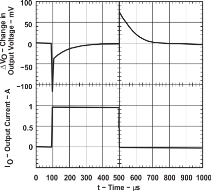
Load transient response | Figure 17, Figure 18 | ||
VO | Output voltage | vs Time | Figure 19 |
Dropout voltage | vs Input voltage | Figure 20 | |
Equivalent series resistance (ESR)(1) | vs Output current | Figure 21–Figure 24 |
VI = 4.3 V | TA = 25°C |
VI = 2.7 V | TA = 25°C |
VI = 3.5 V | TA = 25°C |
VI = 2.7 V |
VI = 4.3 V |
VI = 4.3 V | Co = 10 µF | |
IO = 1 A | TA = 25°C |
IO = 1 A |
CO = 10 µF |
CO = 10 µF | TA = 25°C |
IO = 1 A | ||
VO = 3.3 V | Co = 4.7 µF | |
VI = 4.3 A | TA = 125°C |
VO = 3.3 V | Co = 22 µF | |||
VI = 4.3 A | TA = 125°C |
VI = 4.3 V |
VI = 3.5 V |
VI = 2.7 V |
VI = 4.3 V | Co = 10 µF | TA = 25°C |
CO = 10 µF | TA = 25°C |
CO = 10 µF | IO = 1 A | TA = 25°C |
VO = 3.3 V | Co = 4.7 µF | |
VI = 4.3 A | TA = 25°C |
VO = 3.3 V | Co = 22 µF | |
VI = 4.3 A | TA = 25°C |
The TPS767xx features very low quiescent current, which remains virtually constant even with varying loads. Conventional LDO regulators use a pnp pass element, the base current of which is directly proportional to the load current through the regulator (IB = IC/β). The TPS767xx uses a PMOS transistor to pass current; because the gate of the PMOS is voltage driven, operating current is low and invariable over the full load range.
Another pitfall associated with the pnp-pass element is its tendency to saturate when the device goes into dropout. The resulting drop in β forces an increase in IB to maintain the load. During power up, this translates to large start-up currents. Systems with limited supply current may fail to start up. In battery-powered systems, it means rapid battery discharge when the voltage decays below the minimum required for regulation. The TPS767xx quiescent current remains low even when the regulator drops out, eliminating both problems.
The TPS767xx family also features a shutdown mode that places the output in the high-impedance state (essentially equal to the feedback-divider resistance) and reduces quiescent current to 2 µA. If the shutdown feature is not used, EN should be tied to ground.
The FB pin is an input pin to sense the output voltage and close the loop for the adjustable option . The output voltage is sensed through a resistor divider network to close the loop as shown in Figure 28. Normally, this connection should be as short as possible; however, the connection can be made near a critical circuit to improve performance at that point. Internally, FB connects to a high-impedance wide-bandwidth amplifier and noise pickup feeds through to the regulator output. Routing the FB connection to minimize/avoid noise pickup is essential.
The TPS767xx features a RESET output that can be used to monitor the status of the regulator. The internal comparator monitors the output voltage: when the output drops to between 92% and 98% of its nominal regulated value, the RESET output transistor turns on, taking the signal low. The open-drain output requires a pullup resistor. If not used, it can be left floating. RESET can be used to drive power-on reset circuitry or as a low-battery indicator. RESET does not assert itself when the regulated output voltage falls outside the specified 2% tolerance, but instead reports an output voltage low relative to its nominal regulated value (refer to Figure 1 timing diagram for start-up sequence).
The TPS767xx PMOS-pass transistor has a built-in back diode that conducts reverse currents when the input voltage drops below the output voltage (e.g., during power down). Current is conducted from the output to the input and is not internally limited. When extended reverse voltage is anticipated, external limiting may be appropriate.
The TPS767xx also features internal current limiting and thermal protection. During normal operation, the TPS767xx limits output current to approximately 1.7 A. When current limiting engages, the output voltage scales back linearly until the overcurrent condition ends. While current limiting is designed to prevent gross device failure, care should be taken not to exceed the power dissipation ratings of the package. If the temperature of the device exceeds 150°C(typ), thermal-protection circuitry shuts it down. Once the device has cooled below 130°C(typ), regulator operation resumes.
The TPS767xx family is stable even at zero load; no minimum load is required for operation.
The output voltage of the TPS76701 adjustable regulator is programmed using an external resistor divider as shown in Figure 28. The output voltage is calculated using:
Where: f = 1.1834 V typ (the internal reference voltage)
Resistors R1 and R2 should be chosen for approximately 50-µA divider current. Lower value resistors can be used but offer no inherent advantage and waste more power. Higher values should be avoided as leakage currents at FB increase the output voltage error. The recommended design procedure is to choose R2 = 30.1 kΩ to set the divider current at 50 µA and then calculate R1 using:
NOTE
Information in the following applications sections is not part of the TI component specification, and TI does not warrant its accuracy or completeness. TI’s customers are responsible for determining suitability of components for their purposes. Customers should validate and test their design implementation to confirm system functionality.
The TPS767xx family includes eight fixed-output voltage regulators (1.5 V, 1.8 V, 2.5 V, 2.7 V, 2.8 V, 3.0 V, 3.3 V, and 5.0 V), and an adjustable regulator, the TPS76701 (adjustable from 1.5 V to 5.5 V).
An input capacitor is not usually required; however, a ceramic bypass capacitor (0.047 µF or larger) improves load transient response and noise rejection if the TPS767xx is located more than a few inches from the power supply. A higher-capacitance electrolytic capacitor may be necessary if large (hundreds of milliamps) load transients with fast rise times are anticipated.
Like all low dropout regulators, the TPS767xx requires an output capacitor connected between OUT and GND to stabilize the internal control loop. The minimum recommended capacitance value is 10 µF and the ESR (equivalent series resistance) must be between 50 mΩ and 1.5 Ω. Capacitor values 10 µF or larger are acceptable, provided the ESR is less than 1.5 Ω. Solid tantalum electrolytic, aluminum electrolytic, and multilayer ceramic capacitors are all suitable, provided they meet the requirements described above. Most of the commercially available 10 µF surface-mount ceramic capacitors, including devices from Sprague and Kemet, meet the ESR requirements stated above.
Specified regulator operation is assured to a junction temperature of 125°C; the maximum junction temperature should be restricted to 125°C under normal operating conditions. This restriction limits the power dissipation the regulator can handle in any given application. To ensure the junction temperature is within acceptable limits, calculate the maximum allowable dissipation, PD(max), and the actual dissipation, PD, which must be less than or equal to PD(max).
The maximum-power-dissipation limit is determined using the following equation:
Where:
TJmax is the maximum allowable junction temperature.
RθJA is the thermal resistance junction-to-ambient for the package, i.e., 172°C/W for the 8-terminal SOIC and
RθJA 32.6°C/W for the 20-terminal PWP with no airflow.
TA is the ambient temperature.
The regulator dissipation is calculated using:
Power dissipation resulting from quiescent current is negligible. Excessive power dissipation will trigger the thermal protection circuit.
The table below lists quick access links. Categories include technical documents, support and community resources, tools and software, and quick access to sample or buy.
PARTS | PRODUCT FOLDER | SAMPLE & BUY | TECHNICAL DOCUMENTS | TOOLS & SOFTWARE | SUPPORT & COMMUNITY |
---|---|---|---|---|---|
TPS76715 | Click here | Click here | Click here | Click here | Click here |
TPS76718 | Click here | Click here | Click here | Click here | Click here |
TPS76725 | Click here | Click here | Click here | Click here | Click here |
TPS76727 | Click here | Click here | Click here | Click here | Click here |
TPS76728 | Click here | Click here | Click here | Click here | Click here |
TPS76730 | Click here | Click here | Click here | Click here | Click here |
TPS76733 | Click here | Click here | Click here | Click here | Click here |
TPS76750 | Click here | Click here | Click here | Click here | Click here |
TPS76701 | Click here | Click here | Click here | Click here | Click here |
The following links connect to TI community resources. Linked contents are provided "AS IS" by the respective contributors. They do not constitute TI specifications and do not necessarily reflect TI's views; see TI's Terms of Use.
PowerPAD, E2E are trademarks of Texas Instruments.
All other trademarks are the property of their respective owners.
These devices have limited built-in ESD protection. The leads should be shorted together or the device placed in conductive foam during storage or handling to prevent electrostatic damage to the MOS gates.
SLYZ022 — TI Glossary.
This glossary lists and explains terms, acronyms, and definitions.
The following pages include mechanical, packaging, and orderable information. This information is the most current data available for the designated devices. This data is subject to change without notice and revision of this document. For browser-based versions of this data sheet, refer to the left-hand navigation.
Texas Instruments Incorporated and its subsidiaries (TI) reserve the right to make corrections, enhancements, improvements and other changes to its semiconductor products and services per JESD46, latest issue, and to discontinue any product or service per JESD48, latest issue. Buyers should obtain the latest relevant information before placing orders and should verify that such information is current and complete. All semiconductor products (also referred to herein as "components") are sold subject to TI's terms and conditions of sale supplied at the time of order acknowledgment.
TI warrants performance of its components to the specifications applicable at the time of sale, in accordance with the warranty in TI's terms and conditions of sale of semiconductor products. Testing and other quality control techniques are used to the extent TI deems necessary to support this warranty. Except where mandated by applicable law, testing of all parameters of each component is not necessarily performed.
TI assumes no liability for applications assistance or the design of Buyers' products. Buyers are responsible for their products and applications using TI components. To minimize the risks associated with Buyers' products and applications, Buyers should provide adequate design and operating safeguards.
TI does not warrant or represent that any license, either express or implied, is granted under any patent right, copyright, mask work right, or other intellectual property right relating to any combination, machine, or process in which TI components or services are used. Information published by TI regarding third-party products or services does not constitute a license to use such products or services or a warranty or endorsement thereof. Use of such information may require a license from a third party under the patents or other intellectual property of the third party, or a license from TI under the patents or other intellectual property of TI.
Reproduction of significant portions of TI information in TI data books or data sheets is permissible only if reproduction is without alteration and is accompanied by all associated warranties, conditions, limitations, and notices. TI is not responsible or liable for such altered documentation. Information of third parties may be subject to additional restrictions.
Resale of TI components or services with statements different from or beyond the parameters stated by TI for that component or service voids all express and any implied warranties for the associated TI component or service and is an unfair and deceptive business practice. TI is not responsible or liable for any such statements.
Buyer acknowledges and agrees that it is solely responsible for compliance with all legal, regulatory and safety-related requirements concerning its products, and any use of TI components in its applications, notwithstanding any applications-related information or support that may be provided by TI. Buyer represents and agrees that it has all the necessary expertise to create and implement safeguards which anticipate dangerous consequences of failures, monitor failures and their consequences, lessen the likelihood of failures that might cause harm and take appropriate remedial actions. Buyer will fully indemnify TI and its representatives against any damages arising out of the use of any TI components in safety-critical applications.
In some cases, TI components may be promoted specifically to facilitate safety-related applications. With such components, TI's goal is to help enable customers to design and create their own end-product solutions that meet applicable functional safety standards and requirements. Nonetheless, such components are subject to these terms.
No TI components are authorized for use in FDA Class III (or similar life-critical medical equipment) unless authorized officers of the parties have executed a special agreement specifically governing such use.
Only those TI components which TI has specifically designated as military grade or "enhanced plastic" are designed and intended for use in military/aerospace applications or environments. Buyer acknowledges and agrees that any military or aerospace use of TI components which have not been so designated is solely at the Buyer's risk, and that Buyer is solely responsible for compliance with all legal and regulatory requirements in connection with such use.
TI has specifically designated certain components as meeting ISO/TS16949 requirements, mainly for automotive use. In any case of use of non-designated products, TI will not be responsible for any failure to meet ISO/TS16949.
TI E2E Community : e2e.ti.com
Mailing Address: Texas Instruments, Post Office Box 655303, Dallas, Texas 75265
Copyright© 2014, Texas Instruments Incorporated