TPS780xx 150-mA Low-Dropout Regulator, Ultralow-Power, IQ 500 nA With Pin-Selectable, Dual-Level Output Voltage
1 Features
- Low IQ: 500 nA
- 150-mA, Low-Dropout Regulator With Pin-Selectable Dual Voltage Level Output
- Low Dropout: 200 mV at 150 mA
- 3% Accuracy Over Load, Line, and Temperature
- Available in Dual-Level, Fixed-Output Voltages From 1.5 V to 4.2 V
- Available in an Adjustable Version from 1.22 V to 5.25 V or a Dual-Level Output Version
- VSET Pin Toggles Output Voltage Between Two Factory-Programmed Voltage Levels
- Stable with a 1.0-μF Ceramic Capacitor
- Thermal Shutdown and Overcurrent Protection
- CMOS Logic Level-Compatible Enable Pin
- Available in DDC (TSOT23-5) or DRV (2-mm ×
2-mm SON-6) Package Options
2 Applications
- TI MSP430™ Attach Applications
- Power Rails With Programming Mode
- Dual Voltage Levels for Power-Saving Mode
- Wireless Handsets, Smart Phones, PDAs, MP3 Players, and Other Battery-Operated Handheld Products
3 Description
The TPS780 family of low-dropout (LDO) regulators offer the benefits of ultralow power, miniaturized packaging, and selectable dual-level output voltage levels with the VSET pin.
The ultralow-power and dynamic voltage scaling (DVS) capability which provides dual-level output voltages let designers customize power consumption for specific applications. Designers can now shift to a lower voltage level in a battery-powered design when the microprocessor is in sleep mode, further reducing overall system power consumption. The two voltage levels are preset at the factory and are stored using EPROM and are available on fixed output voltage devices.
The TPS780 series of LDOs are designed to be compatible with the TI MSP430 and other similar products. The enable pin is compatible with standard CMOS logic. The TPS780 series also come with thermal shutdown and current limit to protect the device during fault conditions. All packages have an operating temperature range of TJ = –40°C to 125°C. For more cost-sensitive applications requiring a dual-level voltage option and only on par IQ, consider the TPS781 series, with an IQ of 1.0 μA and dynamic voltage scaling.
Device Information(1)
| PART NUMBER | PACKAGE | BODY SIZE (NOM) |
|---|---|---|
| TPS780xx | SOT (5) | 2.90 mm x 1.60 mm |
| SON (6) | 2.00 mm x 2.00 mm |
- For all available packages, see the orderable addendum at the end of the data sheet.
4 Revision History
Changes from D Revision (September 2012) to E Revision
- Added ESD Ratings table, Feature Description section, Device Functional Modes, Application and Implementation section, Power Supply Recommendations section, Layout section, Device and Documentation Support section, and Mechanical, Packaging, and Orderable Information section Go
- Deleted Dissipation Ratings table; see Thermal InformationGo
- Changed parametric symbol for line and load regulation Go
Changes from C Revision (May 2008) to D Revision
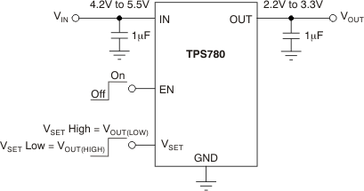
5 Pin Configuration and Functions


Pin Functions
| PIN | I/O | DESCRIPTION | ||
|---|---|---|---|---|
| NAME | SON | SOT | ||
| OUT | 1 | 5 | O | Regulated output voltage pin. A small (1-μF) ceramic capacitor is needed from this pin to ground to assure stability. See Input and Output Capacitor Requirements for more details. |
| N/C | 2 | — | — | Not connected. |
| VSET/FB | 3 | 4 | I | Feedback pin (FB) for adjustable versions; VSET for fixed voltage versions. Drive the select pin (VSET) below 0.4 V to select preset output voltage high. Drive the VSET pin over 1.2 V to select preset output voltage low. |
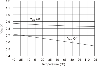
| EN | 4 | 3 | I | Enable pin. Drive this pin over 1.2 V to turn on the regulator. Drive this pin below 0.4 V to put the regulator into shutdown mode, reducing operating current to 18 nA typical. |
| GND | 5 | 2 | — | Ground pin. Tie all ground pins to ground for proper operation. |
| IN | 6 | 1 | I | Input pin. A small capacitor is needed from this pin to ground to assure stability. A typical input capacitor is 1.0 μF. Tie back both input and output capacitor ground to the IC ground, with no significant impedance between them. |
| Thermal pad | — | — | — | (SON package only) Connect the thermal pad to ground. |
6 Specifications
6.1 Absolute Maximum Ratings
over operating free-air temperature range (unless otherwise noted) (1)| MIN | MAX | UNIT | ||
|---|---|---|---|---|
| Voltage | VIN | –0.3 | +6.0 | V |
| VEN and VVSET | –0.3 | VIN + 0.3(2) | ||
| VOUT | –0.3 | VIN + 0.3 | ||
| Current | IOUT | Internally limited | ||
| Output short-circuit duration | Indefinite | |||
| Total continuous power dissipation, PDISS | See Thermal Information | |||
| Temperature | Operating junction, TJ | –40 | 125 | °C |
| Storage, Tstg | –55 | 150 | °C | |
6.2 ESD Ratings
| VALUE | UNIT | |||
|---|---|---|---|---|
| V(ESD) | Electrostatic discharge | Human body model (HBM), per ANSI/ESDA/JEDEC JS-001, all pins(1) | ±2000 | V |
| Charged device model (CDM), per JEDEC specification JESD22-C101, all pins(2) | ±500 | |||
6.3 Recommended Operating Conditions
over operating junction temperature range (unless otherwise noted)| MIN | NOM | MAX | UNIT | ||
|---|---|---|---|---|---|
| VIN | Input voltage | 2.2 | 5.5 | V | |
| VOUT | Output voltage | 1.8 | 4.2 | V | |
| VEN | Enable voltage | 0 | VIN | V | |
| IOUT | Output current | 0 | 150 | mA | |
| TJ | Junction temperature | –40 | 125 | °C | |
6.4 Thermal Information
| THERMAL METRIC(1) | TPS780xx | UNIT | ||
|---|---|---|---|---|
| DDC | DRV | |||
| 5 PINS | 6 PINS | |||
| RθJA | Junction-to-ambient thermal resistance | 193.0 | 65.9 | °C/W |
| RθJC(top) | Junction-to-case (top) thermal resistance | 40.1 | 87.3 | |
| RθJB | Junction-to-board thermal resistance | 34.3 | 35.4 | |
| ψJT | Junction-to-top characterization parameter | 0.9 | 1.7 | |
| ψJB | Junction-to-board characterization parameter | 34.1 | 35.8 | |
| RθJC(bot) | Junction-to-case (bottom) thermal resistance | N/A | 6.1 | |
6.5 Electrical Characteristics
Over operating temperature range (TJ = –40°C to 125°C), VIN = VOUT(nom) + 0.5 V or 2.2 V, whichever is greater; IOUT = 100 μA, VVSET = VEN = VIN, COUT = 1.0 μF, fixed or adjustable, unless otherwise noted. Typical values at TJ = 25°C.| PARAMETER | TEST CONDITIONS | MIN | TYP | MAX | UNIT | |||
|---|---|---|---|---|---|---|---|---|
| VIN | Input voltage range | 2.2 | 5.5 | V | ||||
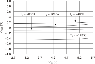
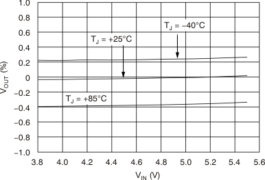
| VOUT(1) | DC output accuracy | Nominal | TJ = 25°C, VSET = high/low | –2% | ±1% | +2% | ||
| Over VIN, IOUT, temperature | VOUT(nom) + 0.5 V ≤ VIN ≤ 5.5 V, 0 mA ≤ IOUT ≤ 150 mA, VSET = high/low |
–3.0% | ±2.0% | +3.0% | ||||
| VFB | Internal reference(9)
(adjustable version only) |
TJ = 25°C, VIN = 4.0 V, IOUT = 75 mA | 1.216 | V | ||||
| VOUT_RANGE | Output voltage range(2)(3)
(adjustable version only) |
VIN = 5.5 V, IOUT = 100 μA(9) | VFB | 5.25 | V | |||
| ΔVOUT(ΔVIN) | Line regulation | VOUT(nom) + 0.5 V ≤ VIN ≤ 5.5 V, IOUT = 5 mA |
–1% | +1% | ||||
| ΔVOUT(ΔIOUT) | Load regulation | 0 mA ≤ IOUT ≤ 150 mA | –2% | +2% | ||||
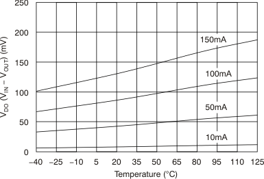
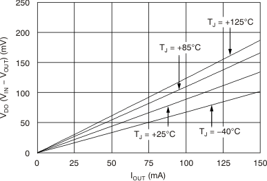
| VDO | Dropout voltage(4) | VIN = 95% VOUT(nom), IOUT = 150 mA | 250 | mV | ||||
| Vn | Output noise voltage | BW = 100 Hz to 100 kHz, VIN = 2.2 V, VOUT = 1.2 V, IOUT = 1 mA |
86 | μVRMS | ||||
| VHI | VSET high (output VOUT(LO) selected), or EN high (enabled) | 1.2 | VIN | V | ||||
| VLO | VSET low (output VOUT(HI) selected), or EN low (disabled) | 0 | 0.4 | V | ||||
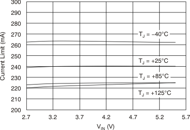
| ICL | Output current limit | VOUT = 0.90 × VOUT(nom) | 150 | 230 | 400 | mA | ||
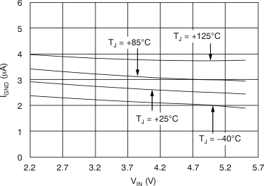
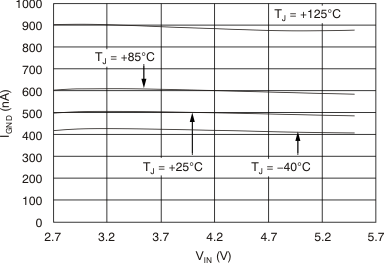
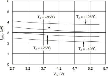
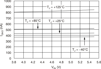
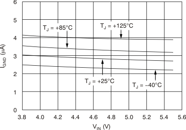
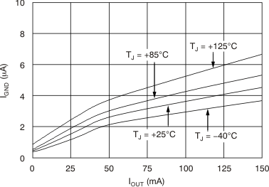
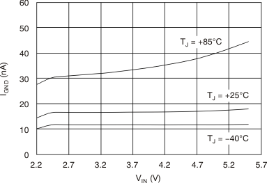
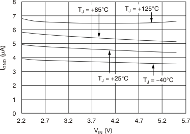
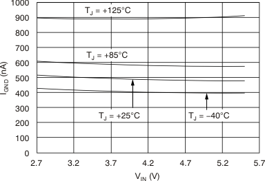
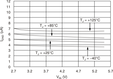
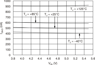
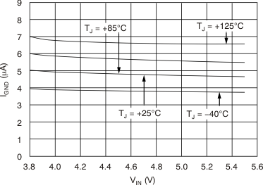
| IGND | Ground pin current | IOUT = 0 mA(5) | 420 | 800 | nA | |||
| IOUT = 150 mA | 5 | μA | ||||||
| ISHDN | Shutdown current (IGND) | VEN ≤ 0.4 V, 2.2 V ≤ VIN < 5.5 V, TJ = –40°C to 100°C |
18 | 130 | nA | |||
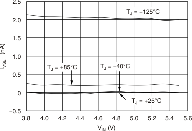
| IVSET | VSET pin current | VEN = VVSET = 5.5 V | 70 | nA | ||||
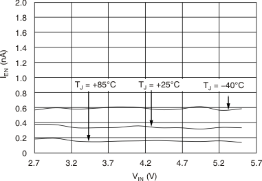
| IEN | EN pin current | VEN = VVSET = 5.5 V | 40 | nA | ||||
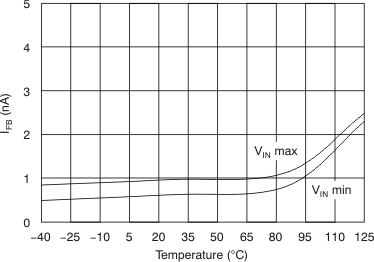
| IFB | FB pin current(10)
(Adjustable version only) |
VIN = 5.5 V, VOUT = 1.2 V, IOUT = 100 μA | 10 | nA | ||||
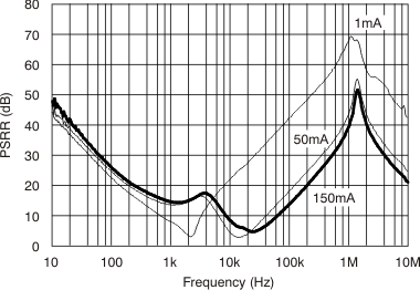
| PSRR | Power-supply rejection ratio | VIN = 4.3 V, VOUT = 3.3 V, IOUT = 150 mA |
f = 10 Hz | 40 | dB | |||
| f = 100 Hz | 20 | |||||||
| f = 1kHz | 15 | |||||||
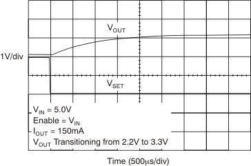
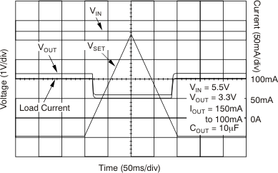
| tTR(H→L) | VOUT transition time (high-to-low) VOUT = 97% × VOUT(HI) |
VOUT_LOW = 2.2 V, VOUT(HI) = 3.3 V, IOUT = 10 mA |
800 | μs | ||||
| tTR(L→H) | VOUT transition time (low-to-high) VOUT = 97% × VOUT(LO) |
VOUT_HIGH = 3.3 V, VOUT(LO) = 2.2 V, IOUT = 10 mA |
800 | μs | ||||
| tSTR | Start-up time(6) | COUT = 1.0 μF, VOUT = 10% VOUT(nom) to VOUT = 90% VOUT(nom) | 500 | μs | ||||
| tSHDN | Shutdown time(7) | IOUT = 150 mA, COUT = 1.0 μF, VOUT = 2.8 V, VOUT = 90% VOUT(nom) to VOUT = 10% VOUT(nom) |
500(8) | μs | ||||
| TSD | Thermal shutdown temperature | Shutdown, temperature increasing | 160 | °C | ||||
| Reset, temperature decreasing | 140 | °C | ||||||
| TJ | Operating junction temperature | –40 | 125 | °C | ||||
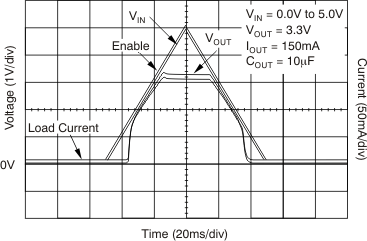
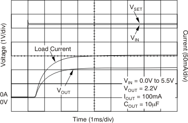
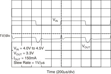
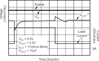
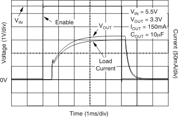
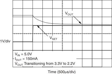
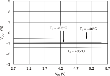
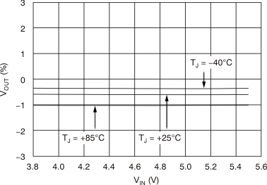
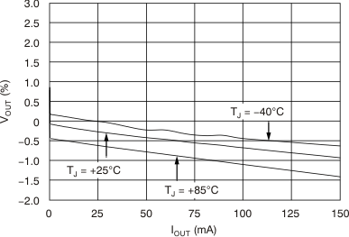
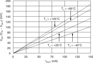
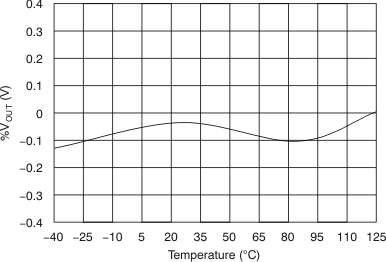
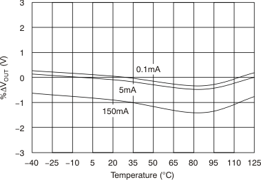
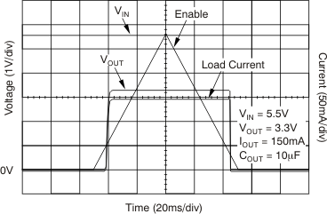
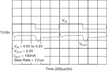
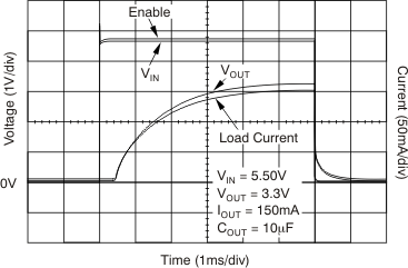
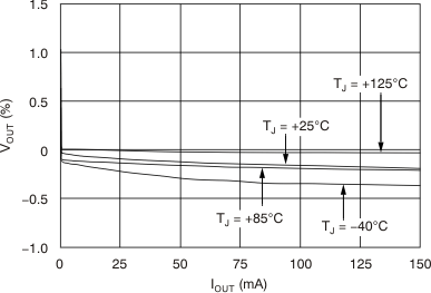
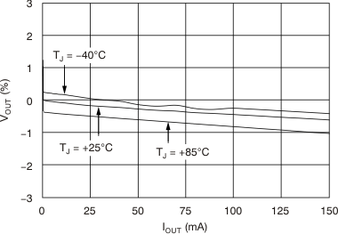
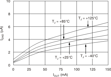
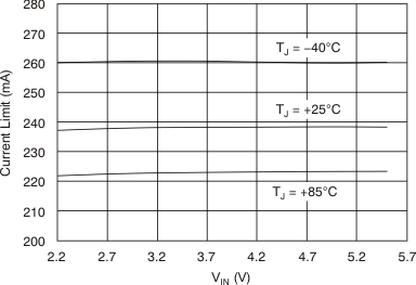
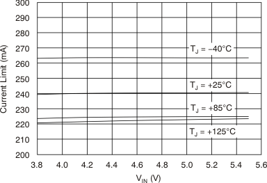
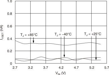
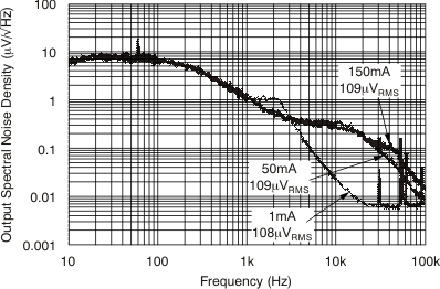
6.6 Typical Characteristics
Over the operating temperature range of TJ = –40°C to 125°C, VIN = VOUT(nom) + 0.5 V or 2.2 V, whichever is greater; IOUT = 100 μA, VEN = VVSET = VIN, COUT = 1 μF, and CIN = 1 μF, unless otherwise noted.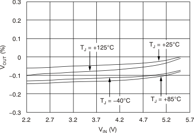
| IOUT = 5 mA | VOUT(nom) = 1.22 V |
| IOUT = 150 mA | VVSET = 1.2 V | VOUT(nom) = 2.2 V |
| IOUT = 150 mA | VVSET = 0.4 V | VOUT(nom) = 3.3 V |
| VVSET = 1.2 V | VIN = 2.7 V | VOUT(nom) = 2.2 V |
| VOUT(nom) = 3.3 V | VIN = 0.95 × VOUT(nom) | |
| VOUT(nom) = 3.3 | VIN = 0.95 × VOUT(nom) | |
| IOUT = 50 mA | VOUT(nom) = 1.22 V |
| IOUT = 0 mA | VVSET = 1.2 V | VOUT(nom) = 2.2 V |
| IOUT = 50 mA | VVSET = 1.2 V | VOUT(nom) = 2.2 V |
| IOUT = 0 mA | VVSET = 0.4 V | VOUT(nom) = 3.3 V |
| IOUT = 50 mA | VVSET = 0.4 V | VOUT(nom) = 3.3 V |
| VVSET = 1.2 V | VIN = 5.5 V | VOUT(nom) = 2.2 V |
| IOUT = 0 mA | VVSET = 0.4 V |
| VVSET = 1.2 V | VOUT = 95% VOUT(nom) | VOUT(nom) = 2.2 V |
| IOUT = 0 mA | VOUT(nom) = 1.22 V |
| IOUT = 100 μA | VVSET = 0.4 V | VOUT(nom) = 3.3 V |
| IOUT = 100 μA | VVSET = 1.2 V | VOUT(nom) = 2.2 V |
| IOUT = 1 mA |
| IOUT = 1 mA | VIN = 3.8 V | VOUT(nom) = 3.3 V |
| VVSET = 0.4 V | VIN = 3.8 V | VOUT(nom) = 3.3 V |
| VIN = 2.7 V | VOUT = 1.2 V | COUT = 2.2 μF |
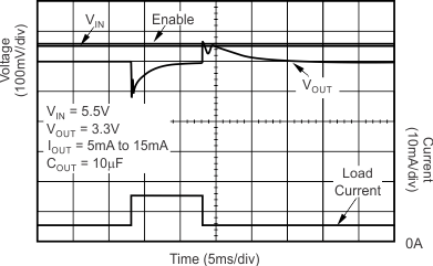
| IOUT = 5 mA | VVSET = 1.2 V | VOUT(nom) = 2.2 V | |
| IOUT = 5 mA | VVSET = 0.4 V | VOUT(nom) = 3.3 V |
| VOUT(nom) = 3.3 V |
| VVSET = 0.4 V | VIN = 3.8 V | VOUT(nom) = 3.3 V |
| VVSET = 0.4 V | VOUT(nom) = 3.3 V | VIN = 0.95 × VOUT(nom) |

| VVSET = 0.4 V | VOUT(nom) = 3.3 V | VIN = 0.95 × VOUT(nom) |
| IOUT = 150 mA | VOUT(nom) = 1.22 V |
| IOUT = 1 mA | VVSET = 1.2 V | VOUT(nom) = 2.2 V |
| IOUT = 150 mA | VVSET = 1.2 V | VOUT(nom) = 2.2 V |
| IOUT = 1 mA | VVSET = 0.4 V | VOUT(nom) = 3.3 V |
| IOUT = 150 mA | VVSET = 0.4 V | VOUT(nom) = 3.3 V |
| VVSET = 0.4 V | VIN = 5.5 V | VOUT(nom) = 3.3 V |
| VOUT = 90% VOUT(nom) | VOUT(nom) = 1.22 V | |
| VVSET = 0.4 V | VOUT = 95% VOUT(nom) | VOUT(nom) = 3.3 V |
| IOUT = 100 μA | VVSET = 1.2 V | VOUT(nom) = 2.2 V |
| IOUT = 1 mA | VOUT(nom) = 1.22 V |
| IOUT = 100 μA | VVSET = 0.4 V | VOUT(nom) = 3.3 V |
| IOUT = 1 mA |
| VVSET = 1.2 V | VIN = 2.7 V | VOUT(nom) = 2.2 V |
| CIN = 1 μF | COUT = 2.2 μF | VVSET = 1.2 V |
| VIN = 2.7 V |