JAJSL23B January 2021 – January 2022 TPS785-Q1
PRODUCTION DATA
- 1 特長
- 2 アプリケーション
- 3 概要
- 4 Revision History
- 5 Pin Configuration and Functions
- 6 Specifications
- 7 Detailed Description
-
8 Application and Implementation
- 8.1 Application Information
- 8.2 Typical Application
- 9 Power Supply Recommendations
- 10Layout
- 11Device and Documentation Support
- 12Mechanical, Packaging, and Orderable Information
パッケージ・オプション
メカニカル・データ(パッケージ|ピン)
サーマルパッド・メカニカル・データ
発注情報
5 Pin Configuration and Functions
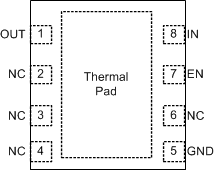
 Figure 5-1 DRB Package
(Fixed),8-Pin VSON(Top View)
Figure 5-1 DRB Package
(Fixed),8-Pin VSON(Top View)Figure 5-3 DRB
Package (Fixed) B Version,8-Pin VSON(Top View)
Figure 5-5 KVU
Package (Fixed),5-Pin TO-252(Top View)
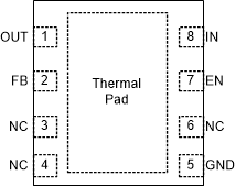
 Figure 5-2 DRB Package
(Adjustable),8-Pin VSON(Top View)
Figure 5-2 DRB Package
(Adjustable),8-Pin VSON(Top View)Figure 5-4 DRB
Package (Adjustable) B Version,8-Pin VSON(Top View)
Figure 5-6 KVU
Package (Adjustable),5-Pin TO-252(Top View)
Table 5-1 Pin Functions
| PIN | I/O | DESCRIPTION | ||||||
|---|---|---|---|---|---|---|---|---|
| NAME | DRB (Fixed) | DRB (Adjustable) | DRB (Fixed) B Version | DRB (Adjustable) B Version | KVU (Fixed) | KVU (Adjustable) | ||
| EN | 7 | 7 | 6 | 6 | 1 | 1 | Input | Enable pin. Driving this pin to logic high enables the device; driving this pin to logic low disables the device. Do not float this pin. If not used, connect EN to IN. |
| FB | — | 2 | — | 2 | — | 5 | Input | Feedback pin. Input to the control-loop error amplifier. This pin is used to set the output voltage of the device with the use of external resistors. Do not float this pin. For adjustable-voltage version devices only. |
| GND | 5 | 5 | 5 | 5 | 3 | 3 | — | Ground pin. This pin must be connected to ground on the board. |
| IN | 8 | 8 | 8 | 8 | 2 | 2 | Input | Input pin. For best performance, place the nominal recommended value or larger ceramic capacitor from IN to GND; see the Recommended Operating Conditions table. Place the input capacitor as close to the input of the device as possible. |
| NC | 2, 3, 4, 6 | 3, 4, 6 | 2, 3, 4, 7 | 3, 4, 7 | 5 | — | — | No connect pin. This pin is not internally connected. Connect to ground for best thermal performance or leave floating. |
| OUT | 1 | 1 | 1 | 1 | 4 | 4 | Output | A 0.47-µF or greater effective capacitance is required from OUT to ground for stability. For best transient response, use a 1-µF or larger ceramic capacitor from OUT to ground. Place the output capacitor as close to output of the device as possible; see the Recommended Operating Conditions table. |
| Thermal Pad | Pad | Pad | Pad | Pad | Pad | Pad | — | The thermal pad is electrically connected to the GND pin. Connect the thermal pad to a large-area GND plane for improved thermal performance. |