JAJSDS1A September 2017 – October 2017 TPS79901-EP
PRODUCTION DATA.
- 1 特長
- 2 アプリケーション
- 3 概要
- 4 改訂履歴
- 5 Pin Configuration and Functions
- 6 Specifications
- 7 Detailed Description
- 8 Application and Implementation
- 9 Power Supply Recommendations
- 10Layout
- 11デバイスおよびドキュメントのサポート
- 12メカニカル、パッケージ、および注文情報
パッケージ・オプション
メカニカル・データ(パッケージ|ピン)
- DRV|6
サーマルパッド・メカニカル・データ
- DRV|6
発注情報
6 Specifications
6.1 Absolute Maximum Ratings
over operating junction temperature range (unless otherwise noted)(1)| MIN | MAX | UNIT | ||
|---|---|---|---|---|
| Voltage(2) | IN | –0.3 | 7 | V |
| EN | –0.3 | VIN + 0.3 | ||
| OUT | –0.3 | VIN + 0.3 | ||
| Current | OUT | Internally limited | mA | |
| Temperature | Operating virtual junction, TJ | –55 | 150 | °C |
| Storage temperature range, Tstg | –55 | 150 | ||
(1) Stresses beyond those listed under Absolute Maximum Ratings may cause permanent damage to the device. These are stress ratings only, which do not imply functional operation of the device at these or any other conditions beyond those indicated under Recommended Operating Conditions. Exposure to absolute-maximum-rated conditions for extended periods may affect device reliability.
(2) All voltages are with respect to network ground terminal.
6.2 ESD Ratings
| VALUE | UNIT | |||
|---|---|---|---|---|
| V(ESD) | Electrostatic discharge | Human-body model (HBM), per ANSI/ESDA/JEDEC JS-001, all pins(1) | ±1500 | V |
| Charged-device model (CDM), per JEDEC specification JESD22-C101, all pins(2) | ±500 | |||
(1) JEDEC document JEP155 states that 500-V HBM allows safe manufacturing with a standard ESD control process.
(2) JEDEC document JEP157 states that 250-V CDM allows safe manufacturing with a standard ESD control process.
6.3 Recommended Operating Conditions
over operating junction temperature range (unless otherwise noted)| MIN | NOM | MAX | UNIT | ||
|---|---|---|---|---|---|
| VIN | Input voltage(1) | 2.7 | 6.5 | V | |
| IOUT | Output current | 0.5 | 200 | mA | |
| TJ | Operating junction temperature | –55 | 125 | °C | |
(1) Minimum VIN = VOUT + VDO or 2.7 V, whichever is greater.
6.4 Thermal Information
| THERMAL METRIC(1) | TPS799 | UNIT | |||
|---|---|---|---|---|---|
| DRV (SON) | |||||
| 6 PINS | |||||
| RθJA | Junction-to-ambient thermal resistance | 74.2 | °C/W | ||
| RθJC(top) | Junction-to-case (top) thermal resistance | 58.8 | °C/W | ||
| RθJB | Junction-to-board thermal resistance | 145.9 | °C/W | ||
| ψJT | Junction-to-top characterization parameter | 0.2 | °C/W | ||
| ψJB | Junction-to-board characterization parameter | 54.4 | °C/W | ||
| RθJC(bot) | Junction-to-case (bottom) thermal resistance | 7.2 | °C/W | ||
(1) For more information about traditional and new thermal metrics, see the IC Package Thermal Metrics application report, SPRA953.
6.5 Electrical Characteristics
at TJ = –55°C to +125°C, VIN = VOUT(nom) + 0.3 V or 2.7 V, whichever is greater; IOUT = 1 mA, VEN = VIN, COUT = 2.2 μF, CNR = 0.01 μF, and VOUT = 3 V (unless otherwise noted). Typical values are at TJ = 25°C.| PARAMETER | TEST CONDITIONS | MIN | TYP | MAX | UNIT | |||
|---|---|---|---|---|---|---|---|---|
| VIN | Input voltage range | 2.7 | 6.5 | V | ||||
| VFB | Internal reference | 1.169 | 1.193 | 1.217 | V | |||
| VOUT | Output voltage range | VFB | 6.5 – VDO | V | ||||
| Output accuracy, nominal | TJ = 25°C | –1% | 1% | |||||
| Output accuracy(1)
over VIN, IOUT, temperature |
VOUT + 0.3 V ≤ VIN ≤ 6.5 V 500 μA ≤ IOUT ≤ 200 mA |
–2% | ±1% | 2% | ||||
| ΔVO(ΔVI) | Line regulation(1) | VOUT(NOM) + 0.3 V ≤ VIN ≤ 6.5 V | 0.02 | %/V | ||||
| ΔVO(ΔIO) | Load regulation | 500 μA ≤ IOUT ≤ 200 mA | 0.002 | %/mA | ||||
| VDO | Dropout voltage(1)
(VIN = VOUT(nom) – 0.1 V) |
IOUT = 200 mA | VOUT(nom) ≤ 3.3 V | 100 | 175 | mV | ||
| VOUT(nom) ≥ 3.3 V | 90 | 160 | ||||||
| ICL | Output current limit | VOUT = 0.9 × VOUT(nom) | 220 | 400 | 600 | mA | ||
| IGND | Ground pin current | 500 μA ≤ IOUT ≤ 200 mA | 40 | 60 | μA | |||
| ISHDN | Shutdown current (IGND) | VEN ≤ 0.4 V, 2.7 V ≤ VIN ≤ 6.5 V | 0.15 | 1 | μA | |||
| IFB | Feedback pin current | –0.5 | 0.5 | µA | ||||
| PSRR | Power-supply rejection ratio | VIN = 3.85 V, VOUT = 2.85 V, CNR = 0.01 μF, IOUT = 100 mA |
f = 100 Hz | 70 | dB | |||
| f = 1 kHz | 66 | |||||||
| f = 10 kHz | 51 | |||||||
| f = 100 kHz | 38 | |||||||
| Vn | Output noise voltage | BW = 10 Hz to 100 kHz, VOUT = 2.85 V | CNR = 0.01 μF | 10.5 × VOUT | μVRMS | |||
| CNR = none | 94 × VOUT | |||||||
| Start-up time | VOUT = 2.85 V, RL = 14 Ω, COUT = 2.2 μF |
CNR = 0.001 μF | 45 | μs | ||||
| CNR = 0.047 μF | 45 | |||||||
| CNR = 0.01 μF | 50 | |||||||
| CNR = none | 50 | |||||||
| VEN(HI) | Enable high (enabled) | 1.2 | VIN | V | ||||
| VEN(LO) | Enable low (shutdown) | 0 | 0.4 | V | ||||
| IEN(HI) | Enable pin current, enabled | VEN = VIN = 6.5 V | 0.03 | 1 | μA | |||
| UVLO | Undervoltage lockout | VIN rising | 1.90 | 2.20 | 2.65 | V | ||
| UVLO hysteresis | VIN falling | 70 | mV | |||||
| Tsd | Thermal shutdown temperature | Shutdown, temperature increasing | 165 | °C | ||||
| Reset, temperature decreasing | 145 | |||||||
(1) VDO is not measured for VOUT(nom) < 2.8 V because minimum VIN = 2.7 V.
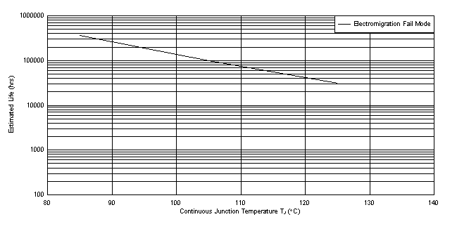
1. See data sheet for absolute maximum and minimum recommended operating conditions.
2. Silicon operating life design goal is 10 years at 105°C junction temperature (does not include package interconnect life).
3. Enhanced plastic product disclaimer applies.
Figure 1. TPS79901-EP Derating Chart
6.6 Typical Characteristics
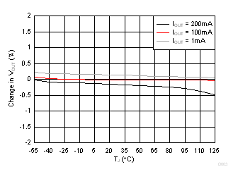
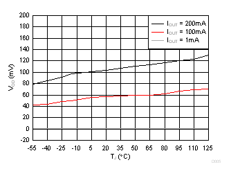
at TJ= –55°C to +125°C, VIN = VOUT(nom) + 0.3 V or 2.7 V, whichever is greater; IOUT = 1 mA, VEN = VIN, COUT = 2.2 μF, CNR = 0.01 μF, and VOUT = 3 V (unless otherwise noted). Typical values are at TJ = 25°C.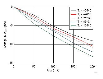
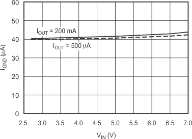
| VOUT = 2.85 V |
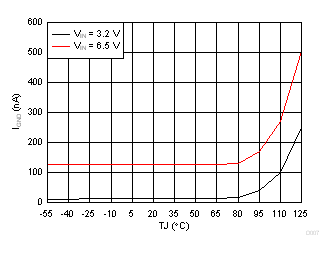
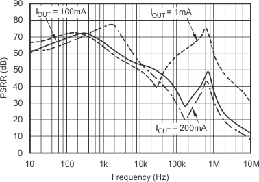
| VIN – VOUT = 0.5 V | VOUT = 2.85 V | |
| CNR = 0.01 µF | COUT = 2.2 µF | |
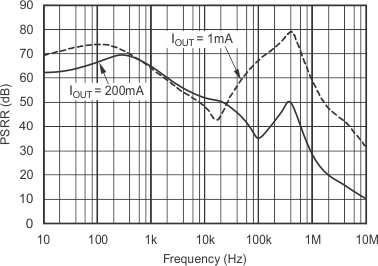
| VIN – VOUT = 1 V | VOUT = 2.85 V | |
| CNR = 0.01 µF | COUT = 10 µF | |
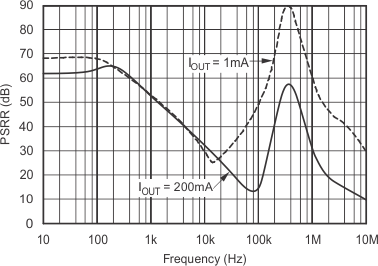
| VIN – VOUT = 1 V | VOUT = 2.85 V | |
| COUT = 10 µF | ||
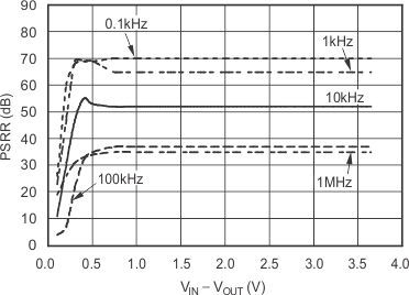
| IOUT = 100 mA | CNR = 0.01 µF | |
| COUT = 2.2 µF | ||
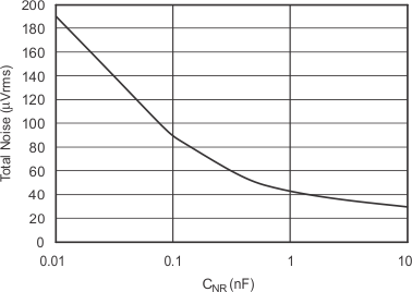
| VOUT = 2.85 V | IOUT = 1 mA | |
| COUT = 2.2 µF | ||
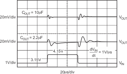
| VOUT = 2.85 V | IOUT = 150 mA | |
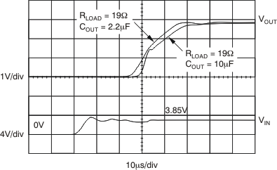
| VEN = VIN | VOUT = 2.85 V | |
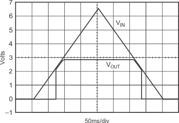
| VOUT = 2.85 V | RL = 19 Ω | |
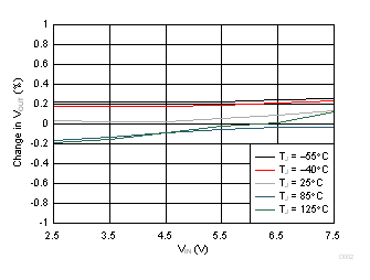
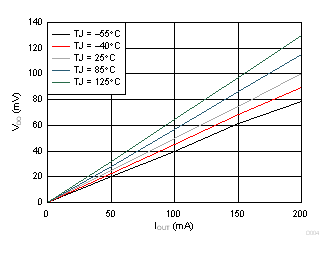
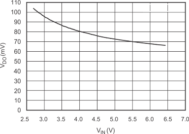
| IOUT = 200 mA |
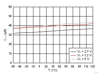
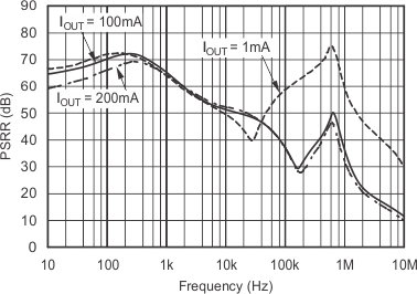
| VIN – VOUT = 1 V | VOUT = 2.85 V | |
| CNR = 0.01 µF | COUT = 2.2 µF | |
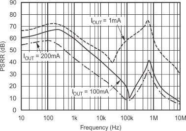
| VIN – VOUT = 0.25 V | VOUT = 2.85 V | |
| CNR = 0.01 µF | COUT = 2.2 µF | |
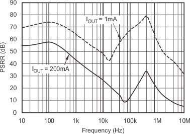
| VIN – VOUT = 0.25 V | VOUT = 2.85 V | |
| CNR = 0.01 µF | COUT = 10 µF | |
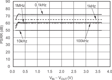
| IOUT = 1 mA | CNR = 0.01 µF | |
| COUT = 2.2 µF | ||
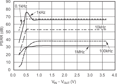
| IOUT = 200 mA | CNR = 0.01 µF | |
| COUT = 2.2 µF | ||
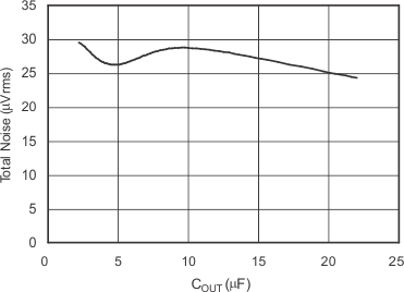
| VOUT = 2.85 V | IOUT = 1 mA | |
| CNR = 0.01 µF | ||
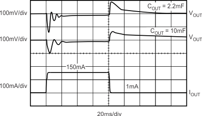
| VIN = 3.35 V | VOUT = 2.85 V | |
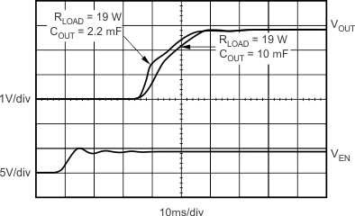
| VIN = 3.85 V | VOUT = 2.85 V | |