JAJSNI3D december 2021 – august 2023 TPS7A14
PRODUCTION DATA
- 1
- 1特長
- 2アプリケーション
- 3概要
- 4Revision History
- 5Pin Configuration and Functions
- 6Specifications
- 7Detailed Description
-
8Application and Implementation
- 8.1
Application Information
- 8.1.1 Recommended Capacitor Types
- 8.1.2 Input, Output, and Bias Capacitor Requirements
- 8.1.3 Dropout Voltage
- 8.1.4 Behavior During Transition From Dropout Into Regulation
- 8.1.5 Device Enable Sequencing Requirement
- 8.1.6 Load Transient Response
- 8.1.7 Undervoltage Lockout Circuit Operation
- 8.1.8 Power Dissipation (PD)
- 8.1.9 Estimating Junction Temperature
- 8.1.10 Recommended Area for Continuous Operation
- 8.2 Typical Application
- 8.3 Power Supply Recommendations
- 8.4 Layout
- 8.1
Application Information
- 9Device and Documentation Support
- Mechanical, Packaging, and Orderable Information
パッケージ・オプション
デバイスごとのパッケージ図は、PDF版データシートをご参照ください。
メカニカル・データ(パッケージ|ピン)
- DRV|6
- YBK|6
サーマルパッド・メカニカル・データ
発注情報
7.3.2 Global Undervoltage Lockout (UVLO)
The TPS7A14 uses two undervoltage lockout circuits: one on the BIAS pin and one on the IN pin to prevent the device from turning on before both VBIAS and VIN rise above their lockout voltages. The two UVLO signals are connected internally through an AND gate, as shown in Figure 7-1, that turns off the device when the voltage on either input is below their respective UVLO thresholds.
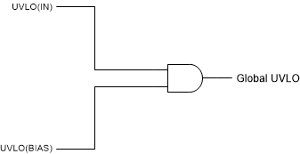
Figure 7-1 Global UVLO circuit