JAJSNI3D december 2021 – august 2023 TPS7A14
PRODUCTION DATA
- 1
- 1特長
- 2アプリケーション
- 3概要
- 4Revision History
- 5Pin Configuration and Functions
- 6Specifications
- 7Detailed Description
-
8Application and Implementation
- 8.1
Application Information
- 8.1.1 Recommended Capacitor Types
- 8.1.2 Input, Output, and Bias Capacitor Requirements
- 8.1.3 Dropout Voltage
- 8.1.4 Behavior During Transition From Dropout Into Regulation
- 8.1.5 Device Enable Sequencing Requirement
- 8.1.6 Load Transient Response
- 8.1.7 Undervoltage Lockout Circuit Operation
- 8.1.8 Power Dissipation (PD)
- 8.1.9 Estimating Junction Temperature
- 8.1.10 Recommended Area for Continuous Operation
- 8.2 Typical Application
- 8.3 Power Supply Recommendations
- 8.4 Layout
- 8.1
Application Information
- 9Device and Documentation Support
- Mechanical, Packaging, and Orderable Information
パッケージ・オプション
デバイスごとのパッケージ図は、PDF版データシートをご参照ください。
メカニカル・データ(パッケージ|ピン)
- DRV|6
- YBK|6
サーマルパッド・メカニカル・データ
発注情報
8.1.10 Recommended Area for Continuous Operation
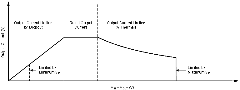
The operational area of an LDO is limited by the dropout voltage, output current, junction temperature, and input voltage. The recommended area for continuous operation for a linear regulator is provided in Figure 8-3 and can be separated into the following regions:
- Dropout voltage limits the minimum differential voltage between the input and the output (VIN – VOUT) at a given output current level; see the Dropout Operation section for more details.
- The rated output current limits the maximum recommended output current level. Exceeding this rating causes the device to fall out of specification.
- The rated junction temperature limits the maximum junction temperature of the device. Exceeding this rating causes the device to fall out of specification and reduces long-term reliability.
- Equation 6 provides the shape of the slope. The slope is nonlinear because the maximum rated junction temperature of the LDO is controlled by the power dissipation across the LDO, thus when VIN – VOUT increases the output current must decrease.
- The rated input voltage range governs both the minimum and maximum of VIN – VOUT.
 Figure 8-3 Continuous
Operation Diagram With Description of Regions