JAJSN43A December 2021 – September 2022 TPS7A21
PRODUCTION DATA
- 1 特長
- 2 アプリケーション
- 3 概要
- 4 Revision History
- 5 Pin Configuration and Functions
- 6 Specifications
- 7 Detailed Description
- 8 Applications and Implementation
- 9 Device and Documentation Support
- 10Mechanical, Packaging, and Orderable Information
パッケージ・オプション
デバイスごとのパッケージ図は、PDF版データシートをご参照ください。
メカニカル・データ(パッケージ|ピン)
- YWD|4
サーマルパッド・メカニカル・データ
発注情報
7.3.5 Foldback Current Limit
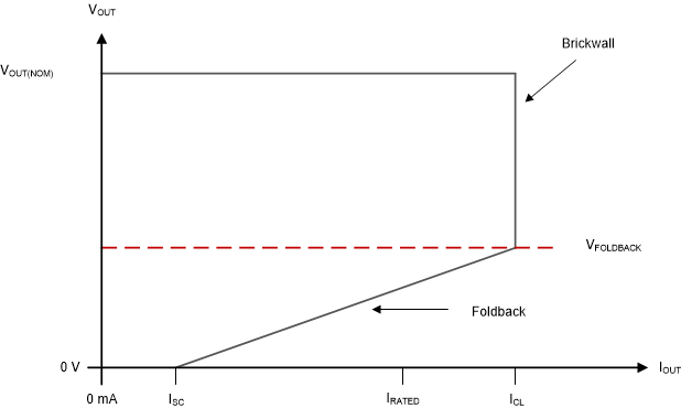
The TPS7A21 has an internal current limit circuit that protects the regulator during transient high-load current faults or shorting events. The current limit is a hybrid brick-wall foldback scheme. The current limit transitions from a brick-wall scheme to a foldback scheme at the foldback voltage (VFOLDBACK).
In a high-load current fault with the output voltage above VFOLDBACK, the brick-wall scheme limits the output current to the current limit (ICL). When the output voltage drops below VFOLDBACK, a foldback current limit activates that scales back the current when the output voltage approaches GND. When the output is shorted, the device supplies a typical current called the short-circuit current limit (ISC). ICL and ISC are listed in the Section 6.5 table.
The output voltage is not regulated when the device is in current limit. When a current limit event occurs, the regulator begins to heat up because of the increase in power dissipation. When the device is in brick-wall current limit, the pass transistor dissipates power [(VIN – VOUT) × ICL]. When the output is shorted and the output voltage is less than VFOLDBACK, the pass transistor dissipates power [(VIN – VOUT) × ISC]. If thermal shutdown is triggered, the device turns off. After the device cools down, the internal thermal shutdown circuit turns the device back on. If the output current fault condition persists, the device cycles between current limit and thermal shutdown. For more information on current limits, see the Know Your Limits application note.
Figure 7-1 shows a diagram of the foldback current limit.
 Figure 7-1 Foldback Current Limit