SBVS163A June 2011 – May 2015 TPS7A3401
PRODUCTION DATA.
- 1 Features
- 2 Applications
- 3 Description
- 4 Revision History
- 5 Pin Configuration and Functions
- 6 Specifications
- 7 Detailed Description
- 8 Application and Implementation
- 9 Power Supply Recommendations
- 10Layout
- 11Device and Documentation Support
- 12Mechanical, Packaging, and Orderable Information
1 Features
- Input Voltage Range: –3 V to –20 V
- Noise:
- 80 μVRMS (10 Hz to 100 kHz)
- Power-Supply Ripple Rejection:
- 50 dB (1 kHz)
- ≥ 27 dB (10 Hz to 1 MHz)
- Adjustable Output:
Approximately –1.18 V to –18 V - Maximum Output Current: 200 mA
- Dropout Voltage: 500 mV at 100 mA
- Stable With Ceramic Capacitors ≥ 2.2 μF
- CMOS Logic-Level-Compatible Enable Pin
- Built-In, Fixed, Current Limit, and Thermal Shutdown Protection
- Available in High Thermal Performance MSOP-8 PowerPAD™ Package
- Operating Temperature Range: –40°C to 125°C
2 Applications
- Cost-Effective Supply Rails for Op Amps, DACs, ADCs, and Other High-Precision Analog Circuitry
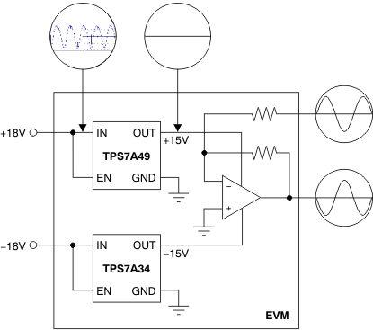
- Cost-Effective Post DC-DC Converter Regulation and Ripple Filtering
3 Description
The TPS7A3401 device is a negative, high-voltage (–20-V), low-noise linear regulator capable of sourcing a maximum load of 200 mA.
These linear regulators include a CMOS logic-level-compatible enable pin. Other features available include built-in current limit and thermal shutdown protection to safeguard the device and system during fault conditions.
The TPS7A3401 is designed using bipolar technology, and is ideal for instrumentation applications where clean voltage rails are critical for improving system performance. This design makes it a cost-effective choice to power operational amplifiers, analog-to-digital converters (ADCs), digital-to-analog converters (DACs), and other analog circuitry.
In addition, the TPS7A3401 linear regulator is suitable for cost-effective, post DC-DC converter regulation. By filtering out the output voltage ripple inherent to DC-DC switching conversion, increased system performance is provided in instrumentation applications.
Device Information(1)
| PART NUMBER | PACKAGE | BODY SIZE (NOM) |
|---|---|---|
| TPS7A3401 | HVSSOP (8) | 3.00 mm × 3.00 mm |
- For all available packages, see the orderable addendum at the end of the data sheet.
Post DC-DC Converter Regulation
