SBVS228B July 2013 – March 2015 TPS7A3501
PRODUCTION DATA.
- 1 Features
- 2 Applications
- 3 Description
- 4 Revision History
- 5 Pin Configuration and Functions
- 6 Specifications
- 7 Detailed Description
- 8 Application and Implementation
- 9 Power Supply Recommendations
- 10Layout
- 11Device and Documentation Support
- 12Mechanical, Packaging, and Orderable Information
パッケージ・オプション
メカニカル・データ(パッケージ|ピン)
- DRV|6
サーマルパッド・メカニカル・データ
- DRV|6
発注情報
7 Detailed Description
7.1 Overview
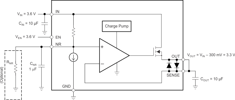
The TPS7A3501 is a positive-voltage, low-noise (3.8-µVRMS) power filter capable of sourcing a 1-A load. Power filters such as the TPS7A3501 provide voltage regulation across the input and output terminals with high accuracy and power-supply rejection ratio. The device is ideally suited as a noise filter for 4.5-V, 3.3-V, and 1.8-V supplies up to 1-A loads.
The input-to-output voltage drop is also user-programmable, from 200 mV up to 500 mV, with an external resistor. If no resistor is used, the TPS7A3501 provides 330 mV of input-to-output voltage regulation.
The TPS7A3501 is stable with 10-µF ceramic input and output capacitors and a 10-nF ceramic noise-reduction capacitor. The device is fully specified over a wide temperature range of –40°C to 125°C and is offered in a low thermal resistance, 2-mm × 2-mm, 6-pin WSON package.
7.3 Feature Description
7.3.1 Power Filter Operation
A power filter is very similar to a low-dropout (LDO) regulator, except that instead of regulating output voltage relative to ground, the power filter regulates output voltage relative to VIN. In other words, a power filter maintains a fixed ΔV from input to output. The device is optimized for high PSRR with a low VIN-to-VOUT delta, leading to a lower power dissipation than standard LDOs. Unlike a standard LDO, the bandgap and noise associated with the device are never gained up, resulting in low output noise regardless of VOUT. The external noise capacitor on the power filter lets the user set the frequency at which the power filter starts to reject noise from the input. Table 1 summarizes the differences between a power filter and a high-performance LDO.
Table 1. Power Filter vs LDO Characteristics
| PARAMETER | POWER FILTER | LDO |
|---|---|---|
| Voltage regulation | Regulates input-to-output delta. Voltage delta can be set from 0.2 V to 0.5 V. Relies on the upstream power rail to set the output voltage. | Regulates the output voltage referenced to ground. Outputs any output voltage within the output voltage range (limited by power dissipation). |
| PSRR | High PSRR at typical switching frequencies of DC-DC converters with lower power dissipation. Lower PSRR at low frequencies. | High PSRR over broad bandwidth. Effective rejection of low-frequency noise and switching noise from DC-DC. |
| Noise | Lower noise, 3.8 µV. Noise is not gained up when VOUT increases. | Low noise (typically in the range of 5 µVRMS to 20 µVRMS). Noise is gained up when VOUT increases. |
| Power dissipation | High PSRR can be achieved with only 330 mV from VIN to VOUT. | Typically requires 750 mV to 1 V of VIN-to-VOUT delta to achieve high PSRR. |
7.3.2 Minimum Load
The device is stable without an output load.
7.3.3 Shutdown
The enable pin (EN) is active high and compatible with standard and low-voltage TTL-CMOS levels. The enable pin voltage level is independent of input voltage and can be biased to a higher value than VIN as long as EN is within the maximum specification. When shutdown capability is not required, EN can be connected to IN.
7.3.4 Internal Current Limit
The device has an internal foldback current limit that helps protect the power filter during fault conditions. The current supplied by the device is gradually reduced when the output voltage decreases. When the output is shorted to GND, the LDO supplies a typical current of 550 mA. When in current limit, the output voltage is not regulated and VOUT = IOUT × RLOAD. For reliable operation, do not operate the device in current limit for extended periods of time.
Because of the nature of the foldback current limit circuitry, if OUT is forced below 0 V before EN goes high, the device may not start up. To ensure proper start-up in applications that have both a positive and negative voltage rail, extra care must be taken to ensure that OUT is greater than or equal to 0 V. There are several ways to help ensure proper start-up for dual-rail applications:
- Enable the device before the negative rail and disable the device after the negative rail.
- Delaying the EN voltage with respect to IN voltage allows the internal pulldown resistor to discharge any residual voltage at OUT.
- If a faster discharge rate is required, or if EN is tied directly to IN, an external resistor from OUT to GND can be used.
7.3.5 Reverse Current
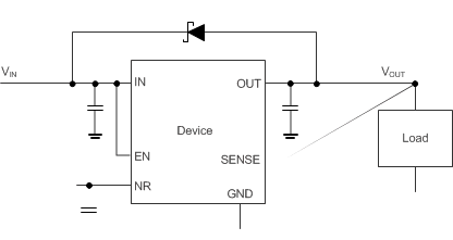
The TPS7A3501 has a built-in body diode that conducts current when the voltage at OUT exceeds the voltage at IN. This current is not internally limited, so if reverse voltage conditions are anticipated, external limiting is required.
If there are potential situations where reverse current is expected, place a diode from OUT to IN, as shown in Figure 20.
 Figure 20. Reverse Current Protection Schematic
7.3.6 Undervoltage Lockout (UVLO)
The device uses an undervoltage lockout circuit to keep the output shut off until the internal circuitry is operating properly, ensuring a well-controlled start-up.
7.3.7 Thermal Protection
Thermal protection disables the output when the junction temperature rises to approximately 160°C, allowing the device to cool. When the junction temperature cools to approximately 140°C, the output circuitry is again enabled. Depending on power dissipation, thermal resistance, and ambient temperature, the thermal protection circuit may cycle on and off. This cycling limits device power dissipation, thus protecting the device from damage resulting from overheating.
Any activation of the thermal protection circuit indicates excessive power dissipation or inadequate thermal dissipation on the PCB. For reliable operation, limit junction temperature to 125°C (maximum). To estimate the margin of safety in a complete design, increase the ambient temperature until the thermal protection is triggered using worst-case loads and signal conditions. For good reliability, thermal protection should trigger at least 35°C above the maximum expected ambient condition of the application. This configuration produces a worst-case junction temperature of 125°C at the highest-expected ambient temperature and worst-case load.
The device internal protection circuitry is designed to protect against overload conditions. This circuitry is not intended to replace proper heat-sinking or thermal dissipation on the PCB. Continuously running the device into thermal shutdown degrades device reliability.
7.4 Device Functional Modes
Table 2 provides a quick comparison between the normal, dropout, and disabled modes of operation.
Table 2. Device Functional Mode Comparison
| OPERATING MODE | PARAMETER | |||
|---|---|---|---|---|
| VIN | EN | IOUT | TJ | |
| Normal | 1.71 ≤ VIN ≤ 5 | VEN > VEN(HI) | IOUT < ICL | TJ < Tsd |
| Disabled | — | VEN < VEN(LO) | — | TJ > Tsd |
7.4.1 Normal Operation
The device functions as a fixed voltage drop filter under the following conditions:
- The input voltage is within the specified operating range of 1.71 V to 5 V.
- The enable voltage has previously exceeded the enable rising threshold voltage and not yet decreased below the enable falling threshold.
- The output current is less than the current limit (IOUT < ICL).
- The device junction temperature is less than the thermal shutdown temperature (TJ < Tsd).
7.4.2 Disabled
The device is disabled under the following conditions:
- The enable voltage is less than the enable falling threshold voltage or has not yet exceeded the enable rising threshold.
- The device junction temperature is greater than the thermal shutdown temperature (TJ > Tsd).
